

Substrate for fabricating superconductive film, superconductive wires and manufacturing method thereof
a superconductive wire and substrate technology, applied in the direction of superconducting magnets/coils, magnetic bodies, instruments, etc., can solve the problem of inability to obtain excellent current characteristics, achieve excellent superconductive characteristics and reliability, avoid delamination, and enhance productivity and manufacturing speed
- Summary
- Abstract
- Description
- Claims
- Application Information
AI Technical Summary
Benefits of technology
Problems solved by technology
Method used
Image

Examples
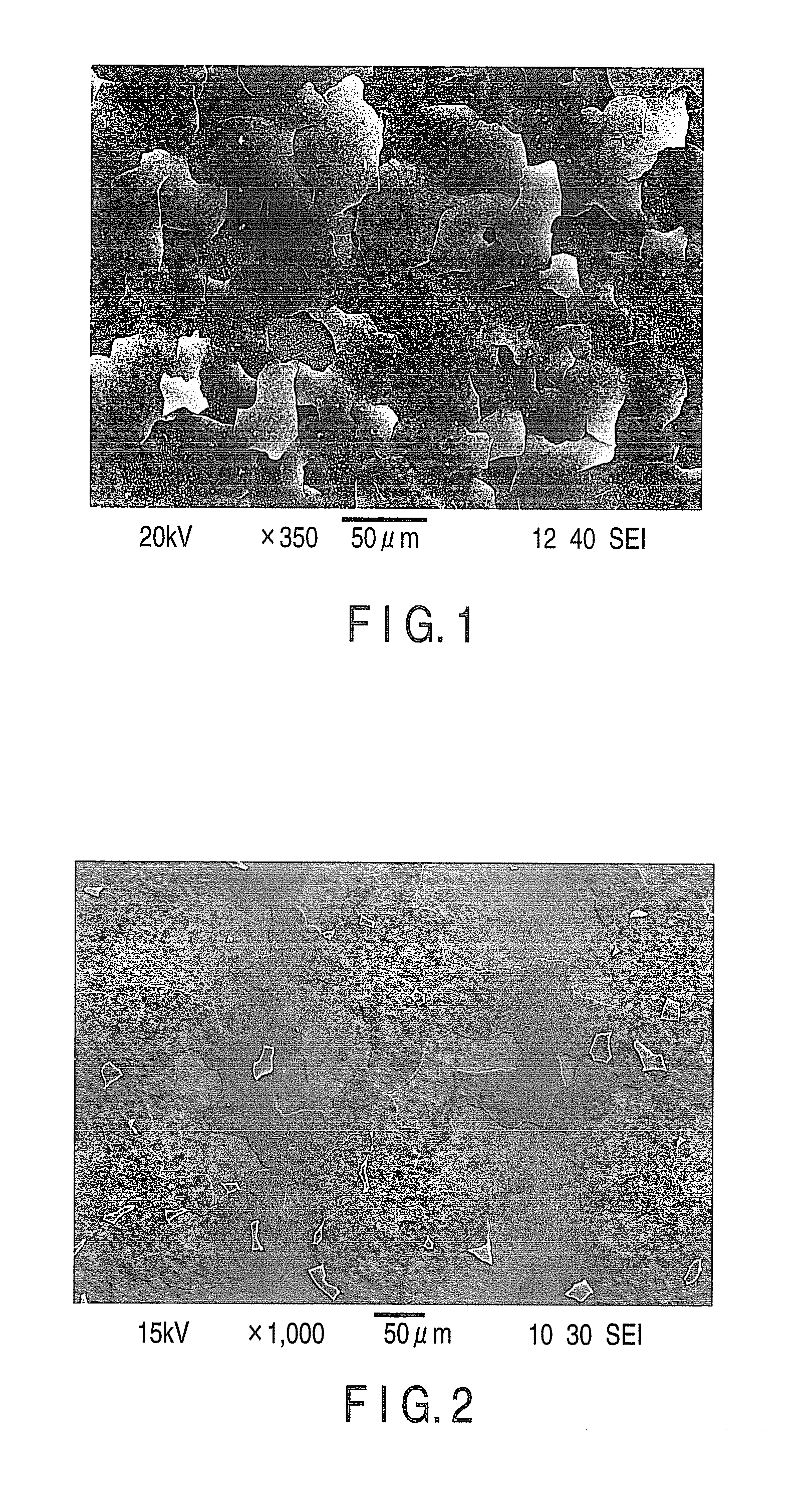
example 1
[0100]A base member made of Ni-based alloy (Hastelloy; trademark: Ni-16Cr-15.6Mo-6Fe-4W-2Co) and roll-worked into a tape-like film having a width of 10 mm and a thickness of 100 μm was employed as a metal substrate. Since a plurality of film fabrication steps to be subsequently applied to this metal substrate include a high-temperature process of about 800° C., a heat-resistant alloy containing elemental Cr was employed for this metal substrate.
[0101]By means of ion beam sputtering method, a Cr layer having a thickness of 50 nm was deposited directly on the surface of the Ni-based alloy base body. Likewise, by means of ion beam sputtering method, a Gd2Zr2O7 layer constituting a first intermediate layer was deposited on the Cr layer under the conditions shown in the following Table 1, thereby preparing a sample.
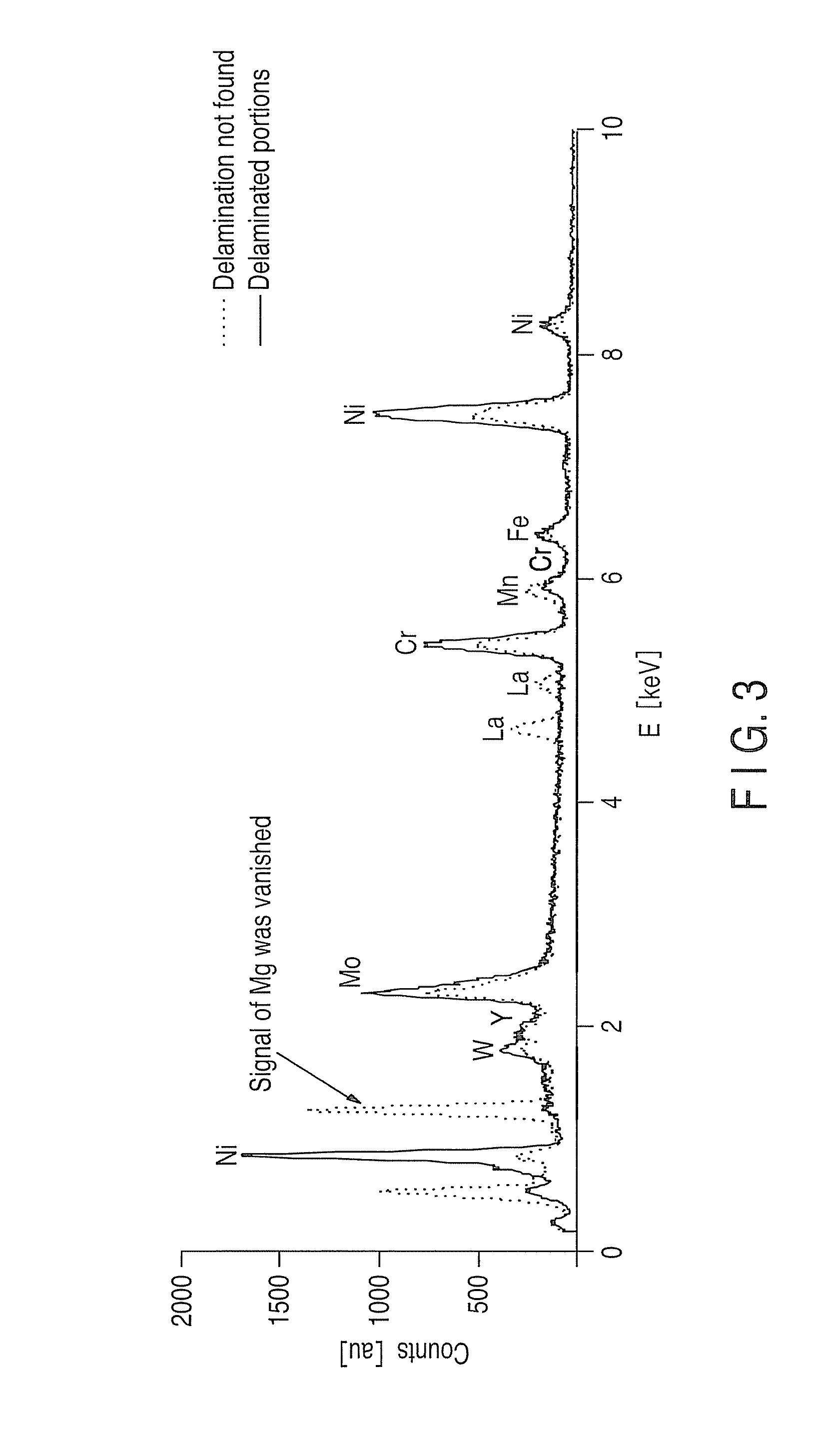
[0102]Subsequently, under the conditions of: 100% oxygen atmosphere and a pressure of 1 atm, the sample was subjected to a heat treatment at a temperature of up to 500° C. The...
example 2
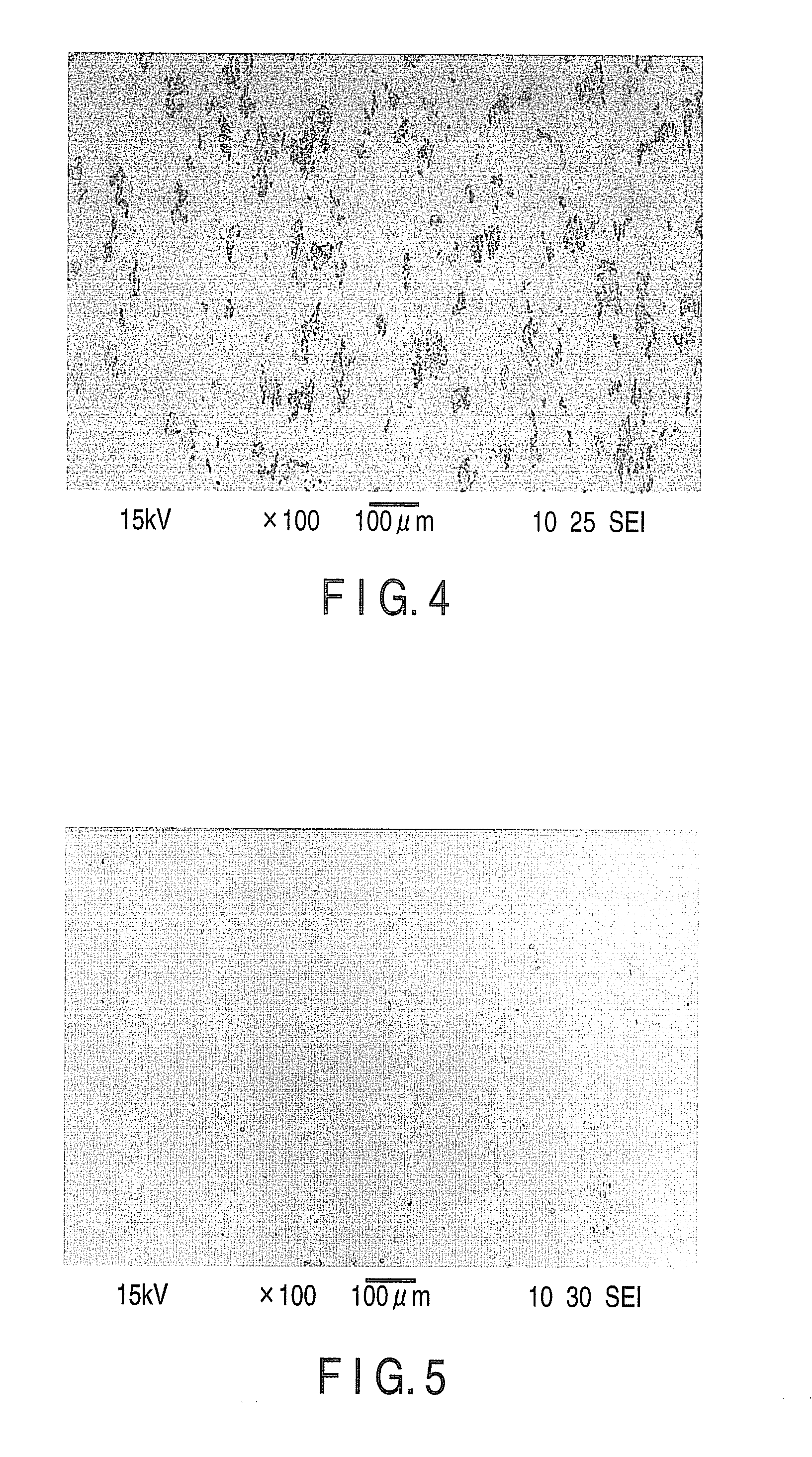
[0107]A base member made of Ni-based alloy (Hastelloy; trademark: Ni-16Cr-15.6Mo-6Fe-4W-2Co) and roll-worked into a tape-like film having a width of 10 mm and a thickness of 100 μm was employed as a metal substrate. Because of the reasons that an oxide layer containing chromium oxide as a major component is to be formed by way of oxygen annealing treatment after depositing an intermediate layer and that a plurality of film fabrication steps to be subsequently applied to this metal substrate include a high-temperature process of about 800° C., a heat-resistant Ni-based alloy containing elemental Cr was employed for this metal substrate. Further, in order to enhance the characteristics for use as an orientated substrate to be used for the manufacture of a superconductive wire, the surface of the metal substrate was polished to have an arithmetic average roughness Ra of 10 nm.
[0108]By means of ion beam sputtering method, a Gd2Zr2O7 layer constituting an intermediate layer was deposited...
example 3
[0113]A base member made of Ni-based alloy (Hastelloy; trademark: Ni-16Cr-15.6Mo-6Fe-4W-2Co) and roll-worked into a tape-like film having a width of 10 mm and a thickness of 100 μm was employed as a metal substrate. Because of the reasons that a plurality of deposition steps to be subsequently applied to this metal substrate include a high-temperature process of about 800° C. and that an oxide layer containing chromium oxide as a major component is enabled to be formed in this high-temperature process, a heat-resistant alloy containing elemental Cr was employed for this metal substrate. Further, in order to enhance the characteristics for use as an orientated substrate to be used for the manufacture of a superconductive wire, the surface of the metal substrate was polished to have an arithmetic average roughness Ra of 10 nm.
[0114]By means of ion beam sputtering method and pulse laser deposition method, an Al2O3 layer and intermediate layers (Y2O3, IBAD-MgO, LaMnO3 and CeO2) were dep...
PUM
| Property | Measurement | Unit |
|---|---|---|
| arithmetic average roughness | aaaaa | aaaaa |
| thickness | aaaaa | aaaaa |
| roughness | aaaaa | aaaaa |
Abstract
Description
Claims
Application Information