

Nitride semiconductor light-emitting device and semiconductor light-emitting device
a light-emitting device and semiconductor technology, applied in semiconductor devices, lasers, semiconductor lasers, etc., can solve the problems of insufficient coupling between surface plasmons, inability to achieve high mg doping concentration, and difficulty in achieving light emission efficiency enhancement effect by beneficial surface plasmons, etc., to achieve good flow of tunneling current, improve light emission efficiency, and reduce drive voltage
- Summary
- Abstract
- Description
- Claims
- Application Information
AI Technical Summary
Benefits of technology
Problems solved by technology
Method used
Image

Examples
first embodiment
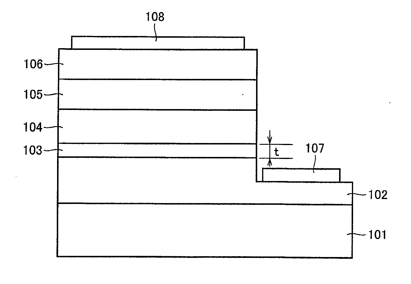
[0058]FIG. 1 shows a schematic cross-sectional view of one example of a nitride semiconductor light-emitting device (a nitride semiconductor light-emitting diode device) according to the present invention. Here, the nitride semiconductor light-emitting device having a construction shown in FIG. 1 includes a substrate 101, a first n-type nitride semiconductor layer 102 formed on substrate 101, a nitride semiconductor layer 103 composed of a nitride semiconductor crystal expressed with a formula AlxGa1−xN (0102, a p-type nitride semiconductor layer 104 formed on nitride semiconductor layer 103, and an active layer 105 formed on p-type nitride semiconductor layer 104.
[0059]In addition, a first n electrode 107 is formed on a surface of first n-type nitride semiconductor layer 102. Moreover, a second n-type nitride semiconductor layer 106 is formed on active layer 105 and a second n electrode 108 is formed on second n-type nitride semiconductor layer 106.
[0060]Here, first n electrode 107...
second embodiment
[0098]FIG. 14 shows a schematic cross-sectional view of a nitride semiconductor light-emitting device (a nitride semiconductor light-emitting diode device) representing one example of the semiconductor light-emitting device according to the present invention. This nitride semiconductor light-emitting device includes a substrate 1401, a first lower layer 1402 formed on substrate 1401 and made of a nitride semiconductor, an intermediate layer 1403 formed on first lower layer 1402 and made of a nitride semiconductor, a second lower layer 1404 formed on intermediate layer 1403 and made of a nitride semiconductor, an active layer 1405 formed on second lower layer 1404 and made of a nitride semiconductor, and an upper layer 1406 formed on active layer 1405 and made of a nitride semiconductor.
[0099]In addition, a first electrode for n-type 1407 is formed in contact with a partially exposed surface of first lower layer 1402, and a second electrode for n-type 1408 is formed in contact with a...
example 1
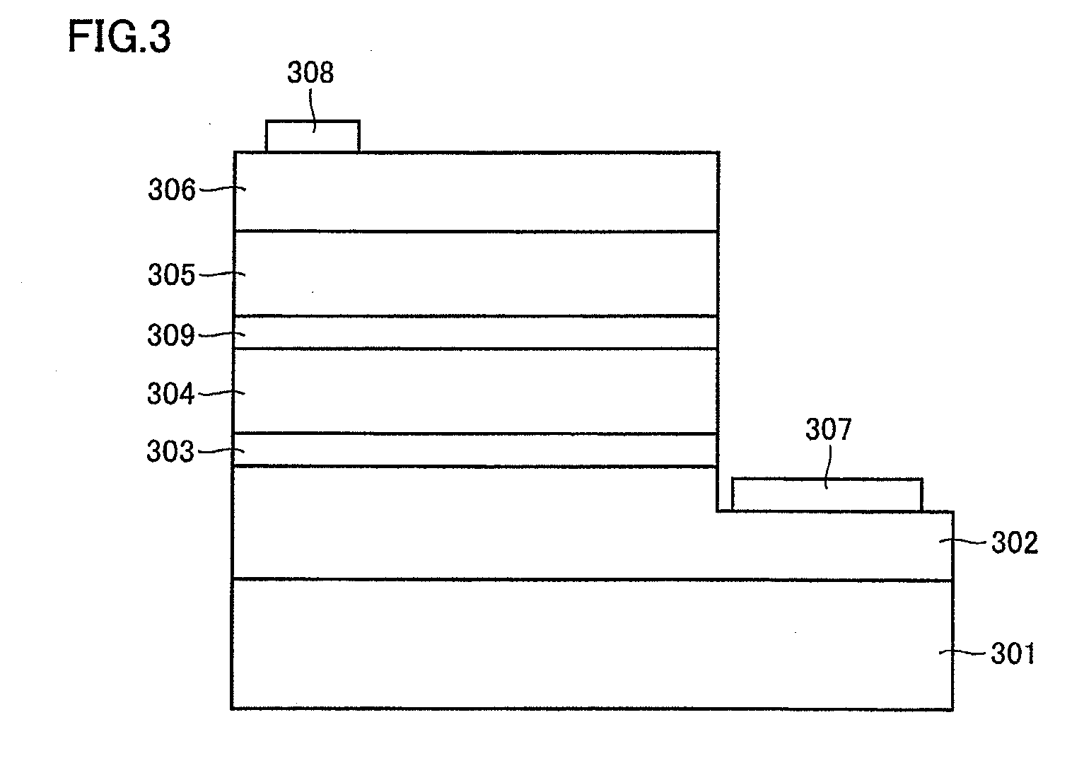
[0136]FIG. 3 shows a schematic cross-sectional view of a nitride semiconductor light-emitting diode device according to Example 1 representing one example of the nitride semiconductor light-emitting device according to the present invention. Here, the nitride semiconductor light-emitting diode device according to Example 1 has such a construction that a first n-type GaN layer 302 having a thickness of 5 μm, an AlN intermediate layer 303 having a thickness of 2.5 nm, a p-type GaN layer 304 having a thickness of 0.3 μm, a p-type Al0.1Ga0.9N carrier blocking layer 309 having a thickness of 10 nm, a multiple quantum well active later 305 having a thickness of 0.168 μm, and a second n-type GaN layer 306 having a thickness of 0.3 μm are stacked in this order on a sapphire substrate 301 having a thickness of 400 μm, in which a first n electrode 307 is formed on first n-type GaN layer 302 and a second n electrode 308 is formed on second n-type GaN layer 306.
[0137]Here, multiple quantum well...
PUM
 Abstract
Description
Claims
Application Information