Plasma mediated ashing processes

a technology of plasma and ashing, applied in the field of plasma mediated ashing processes, can solve the problems of unsatisfactory changes, damaged, photoresist removal process, etc., and achieve the effect of suppressing and/or reducing fast diffusing species

Inactive Publication Date: 2011-09-22
LAM RES CORP
View PDF23 Cites 23 Cited by
  • Summary
  • Abstract
  • Description
  • Claims
  • Application Information

AI Technical Summary

Benefits of technology

In one embodiment, a plasma ashing process for removing photoresist, polymers and / or residues from a substrate comprises placing the substrate including the photoresist, polymers, and / or residues into a reaction chamber; generating a plasma from a gas mixture comprising oxygen gas (O2) and / or an oxygen containing gas; suppressing and / or reducing fast diffusing species in the plasma; and exposing the substrate to the plasma to selectively remove the photoresist, polymers, and / or residues from the substrate, wherein the plasma is substantially free from fast diffusing species.

Problems solved by technology

Typically, sensitive substrate materials such as silicon implanted with very shallow dopants, SiGe, high-k dielectrics, metal gates, and the like are exposed during the photoresist removal process and can become damaged during the photoresist removal process.
The substrate damage may generally be in the form of substrate erosion (e.g., physical removal of a portion of the substrate caused by etching, sputtering, and the like, e.g., silicon loss), substrate oxidation, dopant bleaching / concentration changes, or combinations thereof These changes are undesirable as they will change the electrical, chemical, and physical properties of the substrate.
Moreover, small deviations in the patterned profiles formed in the underlayers can adversely impact device performance, yield, and reliability of the final integrated circuit.
For example, excessive silicon loss can deleteriously alter electrical current saturation at a given applied voltage as well as result in parasitic leakage due to decreased junction depth detrimentally altering electrical functioning of the device.
Current plasma mediated ashing processes are generally unsuitable for this type of application.
However, oxygen based plasma processes can result in significant amounts of substrate surface oxidation, typically on the order of about 10 angstroms or more.
Because silicon loss is generally known to be governed by silicon surface oxidation for plasma resist stripping processes, the use of oxygen (O2) based plasma ashing processes is considered by many to be unacceptable for the 32 nm and beyond technology nodes for advanced logic devices, where almost “zero” substrate loss is required and new materials are being introduced such as embedded SiGe source / drain, high-k gate dielectrics, metal gates and NiSi contact which are extremely sensitive to surface oxidation.
Likewise, it has been found that traditional fluorine containing plasma processes, in addition to unacceptable substrate loss, often results in dopant bleaching.
Other FEOL plasma ashing processes use reducing chemistries such as forming gas (N2 / H2), which provides good results as it relates to substrate oxidation but has throughput issues because of its lower resist removal rates.
Moreover, hydrogen based plasmas have often been found to induce changes to the dopant distribution, which deleteriously affects the electrical properties of the device.
Because of this, prior plasma mediated ashing processes are generally considered unsuitable for removing photoresist in the FEOL process flow for the advanced design rules.
Consequently, much attention has been directed to wet chemical removal of photoresist because of what is perceived as insurmountable problems associated with plasma mediated ashing for these design rules, e.g., substrate loss, dopant bleaching, and the like.

Method used


Image

  • Plasma mediated ashing processes
  • Plasma mediated ashing processes
  • Plasma mediated ashing processes

Examples


example 1

In this example, photoresist coated onto a silicon substrate was exposed to a nitrous oxide stripping chemistry in a RapidStrip320 plasma ashing tool commercially available from Axcelis Technologies, Inc. The photoresist was an i-line photoresist and was deposited onto the silicon substrate at a thickness of 1.9 microns. The plasma chemistry was formed by flowing nitrous oxide gas at 7 standard liters per minute (slm) into the plasma ashing tool at a pressure of 1 Torr, a temperature of 240° C., and a power setting of 3500 Watts.

Ashing rate, cross wafer uniformity, and oxide growth of the nitrous oxide plasma stripping process was compared with oxygen-free reducing plasma (forming gas) and an oxygen based plasma. The reducing plasma was formed from a gas mixture of forming gas (3% hydrogen in nitrogen) at a flow rate of 7 slm into the plasma ashing tool at a pressure of 1 Torr, a temperature of 240° C. and a power setting of 3500 Watts. The oxygen based plasma was formed using 90% o...

example 2

In this example, a small amount of CF4 was added to different plasma gas mixtures and processed in the RapidStrip320 plasma ashing tool. Silicon substrates were exposed to the different plasma chemistries and oxide growth was measured. The results are shown in Table 1 below. In each instance, the various plasmas were formed using a flow rate of the gas mixture of 7 slm into the plasma ashing tool at a pressure of 1 Torr, and a power setting of 3500 Watts.

TABLE 1Process TimeOxide GrowthPlasma Chemistry(seconds)(Å)CF4 / N2O1033.24CF4 / 3%O2 / Forming Gas1039.54CF4 / 90%O2 / Forming Gas1038.763%O2 / Forming Gas1409.82

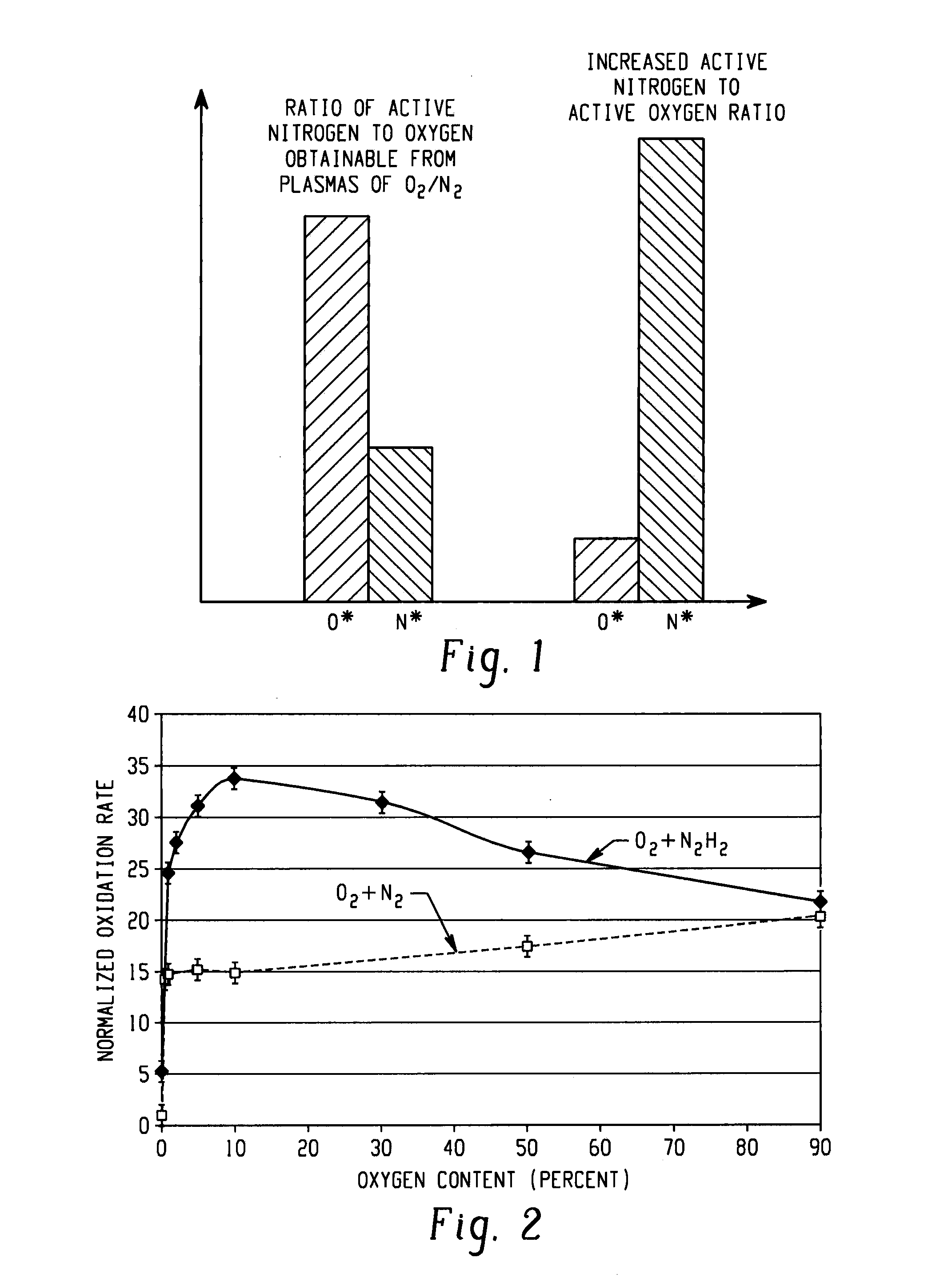
As shown, the addition of small amounts of CF4 during formation of the plasma resulted in minimal substrate loss as evidenced by the oxide growth, and advantageously, can be expected to produce more energetic species, which should effectively increase the ashing rate relative to the results observed in Example 1. The plasma of CF4 / N2O had the highest active nitrogen to active oxygen r...

example 3

In this example, substrate damage was measured using the RapidStrip320 plasma ashing tool in terms of silicon loss, oxide growth and oxide loss for a plasma formed from nitrous oxide (i.e., labeled as new technology), which was compared to prior art plasmas formed from O2 / forming gas mixtures with and without a small amount of carbon tetrafluoride. The forming gas composition was 3% hydrogen in nitrogen. The results are graphically shown in FIG. 5A. In each instance, the various plasmas were formed using a flow rate of the gas mixture of 7 slm into the plasma ashing tool at a pressure of 1 Torr, a temperature of 240° C. and a power setting of 3500 Watts. The substrate damage included (i) silicon loss from silicon-on-insulator (SOT) test structures, (ii) silicon-oxide growth on bare silicon test wafers and silicon-oxide loss from silicon thermal oxide test wafers. Panels (b) and (c) compare scanning electron micrograph images of a post p-MOS high-dose ion implant cleaning application...


PUM

PropertyMeasurementUnit
temperatureaaaaaaaaaa
power densityaaaaaaaaaa

Abstract

A plasma ashing process for removing photoresist, polymers and / or residues from a substrate comprises placing the substrate including the photoresist, polymers, and / or residues into a reaction chamber; generating a plasma from a gas mixture comprising oxygen gas (O2) and / or an oxygen containing gas; suppressing and / or reducing fast diffusing species in the plasma; and exposing the substrate to the plasma to selectively remove the photoresist, polymers, and / or residues from the substrate, wherein the plasma is substantially free from fast diffusing species.

Description

BACKGROUND OF THE INVENTIONThe present disclosure generally relates to plasma mediated ashing processes that provide effective removal of organic materials from a semiconductor substrate while enabling reduced substrate oxidation and / or erosion during processing, and more particularly, to plasma mediated ashing processes wherein the plasma is substantially free of fast diffusing species.The integrated circuit manufacturing process can generally be divided into front end of line (FEOL) and back end of line (BEOL) processing. The FEOL processes are focused on fabrication of the different devices that make up the integrated circuit, whereas BEOL processes are generally focused on forming metal interconnects between the different devices of the integrated circuit. Examining the International Technology Roadmap for Semiconductors (ITRS) for FEOL processing reveals critical performance challenges faced by future devices in a number of key areas including plasma ashing. For example, the ro...

Claims


Application Information

Patent Timeline
Patent Type & Authority Applications(United States)
IPC IPC(8): B08B7/00B08B13/00C23F1/08
CPCG03F7/427H01L21/02101H01L21/31138
Inventor BERRY, IVAN L.WALDFRIED, CARLOLUO, SHIJIANESCORCIA, ORLANDO
Owner LAM RES CORP
Why Eureka
Try Eureka