Electrophoretic deposition and reduction of graphene oxide to make graphene film coatings and electrode structures
a graphene film and electrode structure technology, applied in the field of graphene materials, can solve the problems of ineffective large-area material production methods, undesirable limitations in the preparation method, and limited films produced by membrane filtration methods
- Summary
- Abstract
- Description
- Claims
- Application Information
AI Technical Summary
Benefits of technology
Problems solved by technology
Method used
Image
Examples
example 1
[0066]In a first example, a graphite oxide sample was prepared using a modified Hummer's method. 500 mg of natural graphite (SP-1, available from Bay Carbon) was mixed with 20 ml of concentrated H2SO4 in a flask, followed by the addition of 1.75 g of KMnO4 over a 15 minute period; during addition of KMnO4 the mixture was stirred with a Teflon-coated stirring bar while positioned in a water bath at room temperature. After addition of KMnO4, the mixture was heated at 35° C. and stirred for 2 hours. An ice bath was then used to cool down the solution to about 3-4° C., after which 23 ml of deionized water was slowly added into the flask while stifling to minimize heating. The temperature in the ice bath was monitored and controlled to be no higher than 7° C. by adding ice and controlling the addition of deionized water. Once the temperature was stabilized, more deionized water (270 ml) was added to further dilute the suspension. The suspension was continuous...
example 2
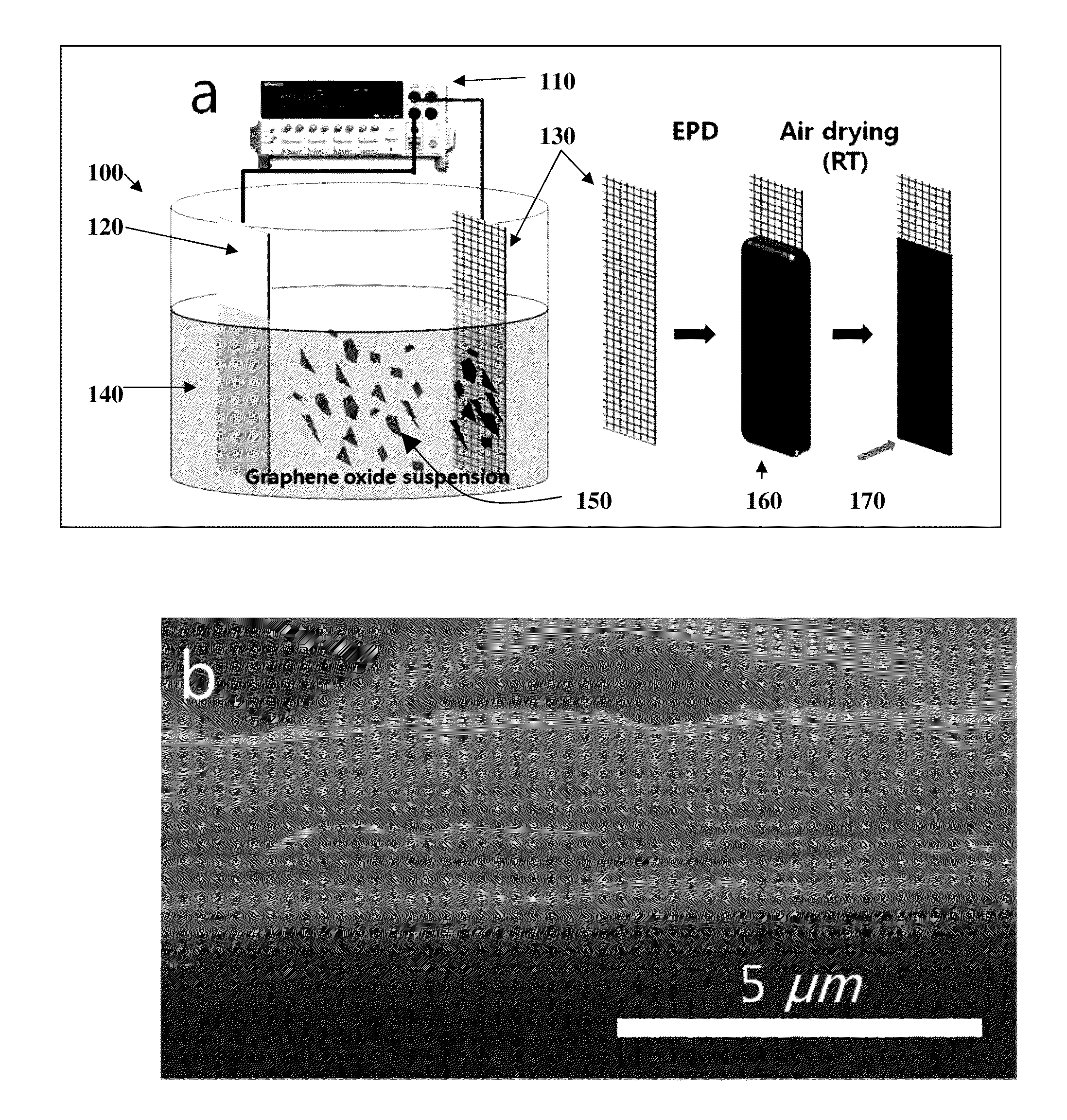
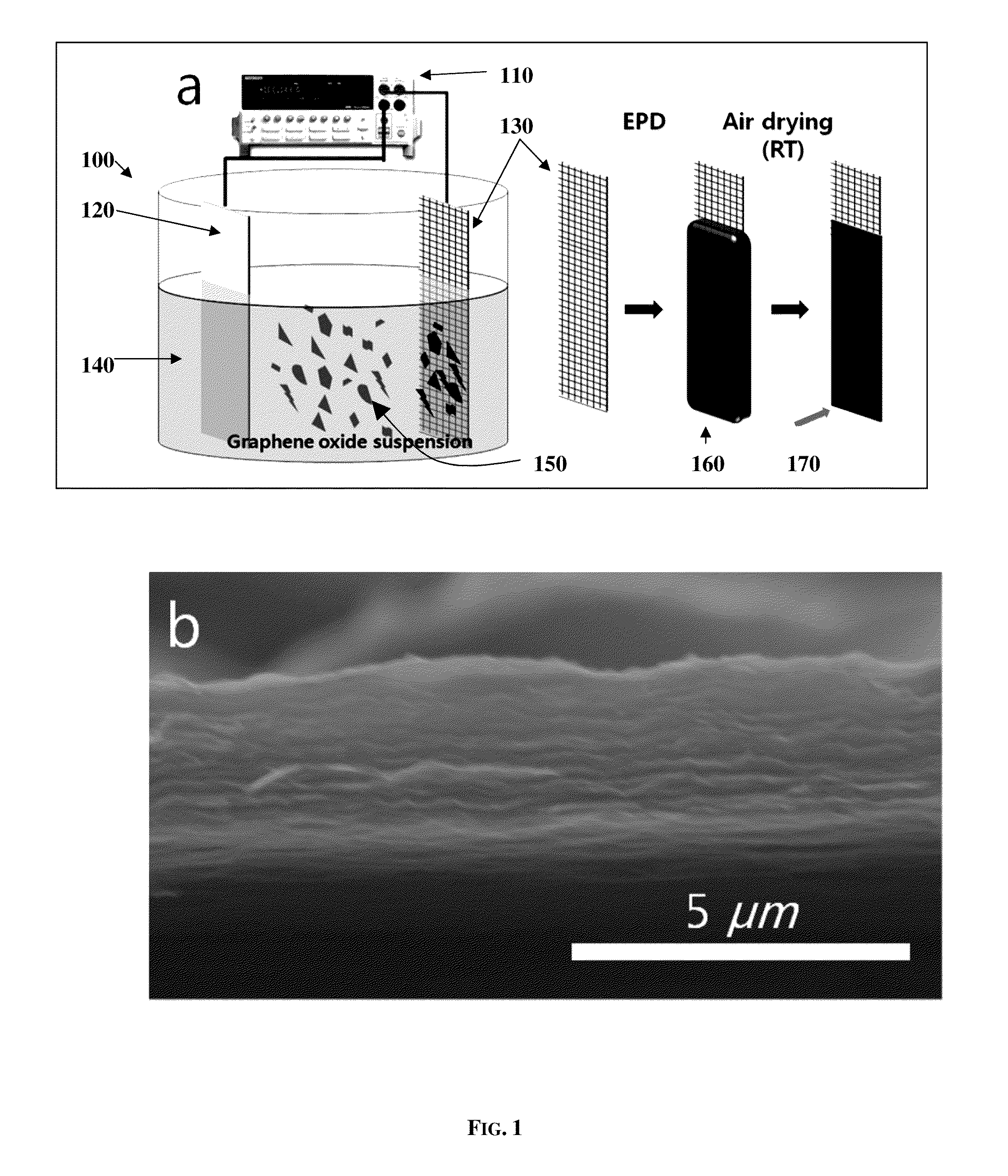
[0067]In a second example, graphene oxide (G-O) was deposited using electrophoretic deposition techniques. For the electrophoretic deposition (EPD), the graphite oxide (GO) was first dispersed in water and sonicated (VWR B2500A-MT) for 2 h at room temperature. A uniform and stable suspension in water containing 1.5 mg / mL of graphene oxide (G-O) platelets was obtained.
[0068]A 200 mesh stainless steel substrate (3×5 cm) was then used as a positive electrode (anode). Other materials, such as, for example, aluminum foil, copper plate, nickel plate, and Si wafer substrates have also been used as anode materials. The electrodes were vertically oriented and separated by 1 cm in a beaker containing the G-O suspension. A direct-current voltage was then applied in the range of 1-40 V (Keithley 6613C DC power supply), with deposition times ranging from 1 to 10 min. After deposition, samples were air-dried at room temperature for 24 h.
example 3
Characterization of Films
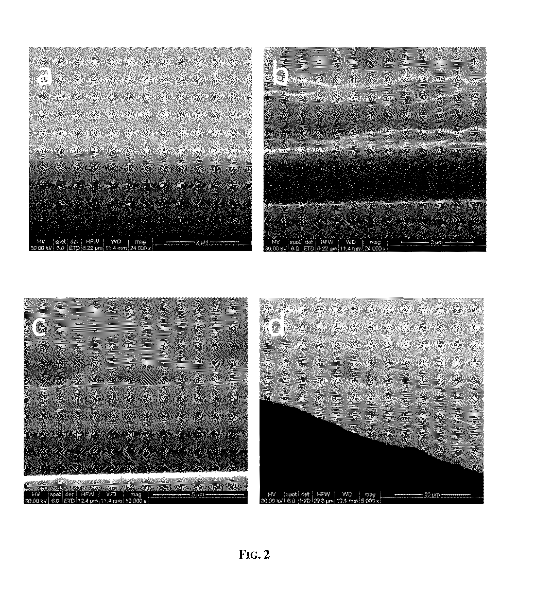
[0069]In a third example, electrophoretically deposited films were characterized. Raman measurements were made using a WiTec Alpha300 confocal Raman microscope with a 532 nm line from a frequency-doubled Nd:Yag laser. The electrical conductivity of the deposited films was measured by the van der Pauw method (using a Keithley 6221 DC and AC current source, and two electrometers, both Keithley 6514). Elemental analysis was also performed on the resulting ‘G-O paper’ and ‘EPD-gO film’ samples. A FEI Quanta-600 FEG Environmental SEM was used to obtain the cross-sectional image of the EPD-gO film. The thermogravimetric analysis (TGA) of paper samples was measured with a PERKIN-ELMER TGA with a heating rate of 1° C. / min in nitrogen. XRD of the EPD-gO film was measured from 5° to 50° (two theta) in part to obtain the mean interlayer spacing of the stacked and overlapped platelets (Phillips APD 3520 powder X-ray diffractometer with Cu K-alpha radiation (40 keV, 30 m...
PUM
| Property | Measurement | Unit |
|---|---|---|
| voltage | aaaaa | aaaaa |
| concentration | aaaaa | aaaaa |
| concentration | aaaaa | aaaaa |
Abstract
Description
Claims
Application Information


