
Heat treatment method of znte single crystal substrate and znte single crystal substrate

a single crystal substrate and heat treatment technology, applied in the direction of crystal growth process, polycrystalline material growth, after treatment details, etc., can solve the problems of high te, low light transmission of znte single crystal substrate, and difficulty in growing bulk crystals by traditional manufacture techniques. , to achieve the effect of reducing the temperature of the substrate, high light transmission, and superior characteristi

Inactive Publication Date: 2011-09-29
ASAHI TOSHIAKI +2
View PDF2 Cites 0 Cited by
  • Summary
  • Abstract
  • Description
  • Claims
  • Application Information

AI Technical Summary

Benefits of technology

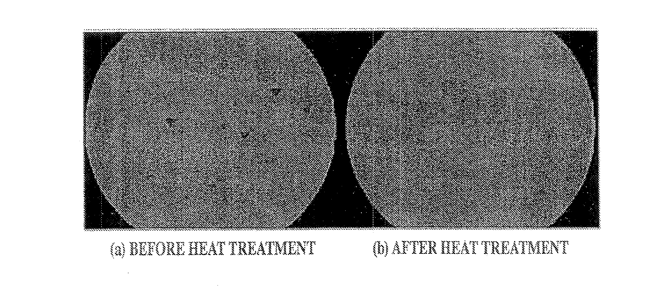
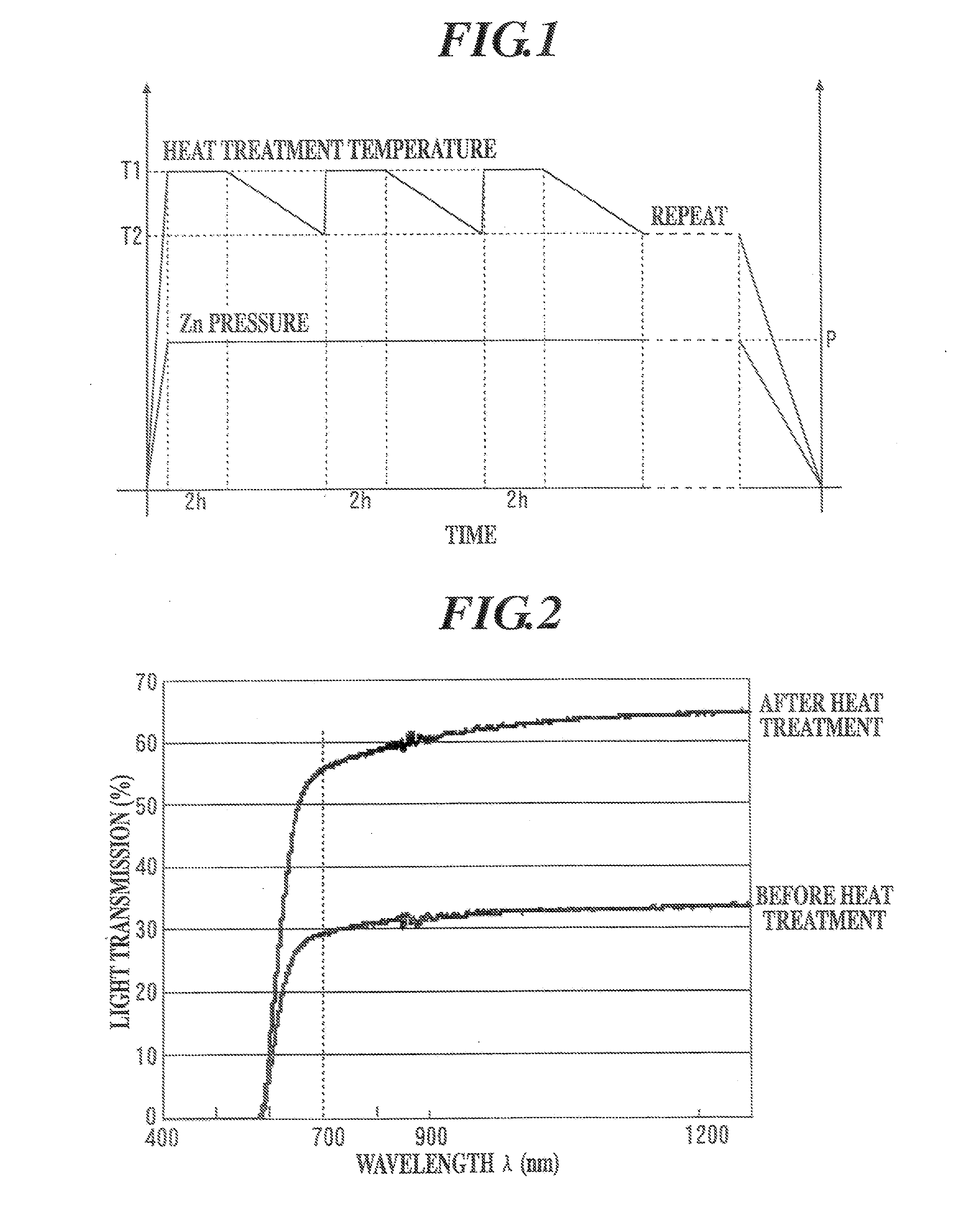
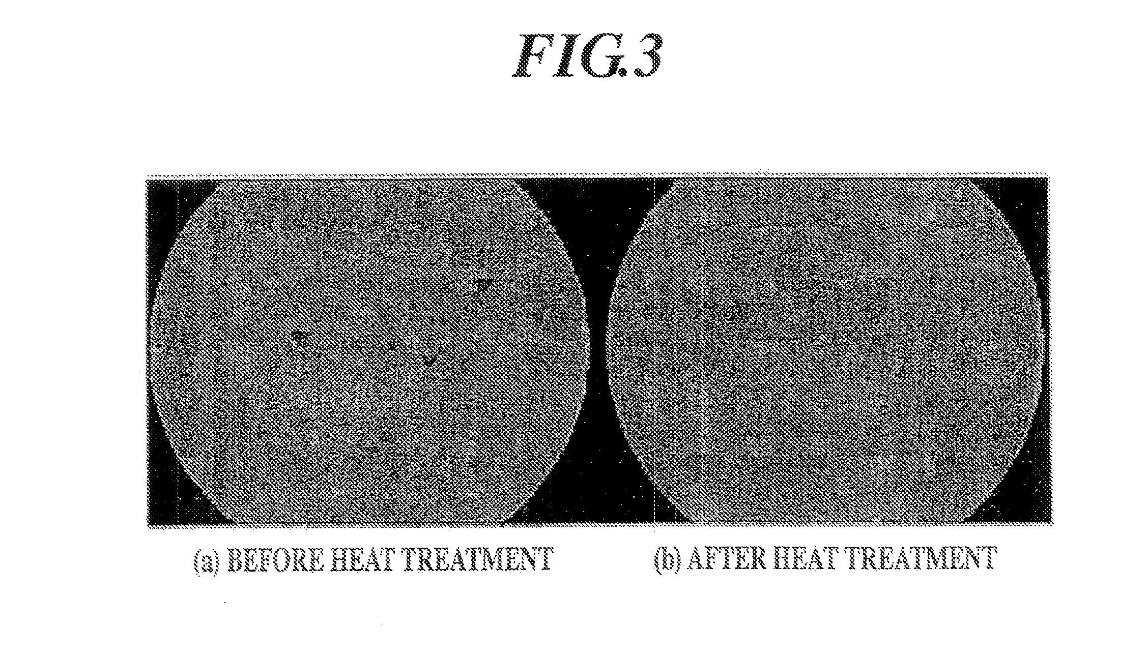
The method achieves a light transmission of 50% or more for wavelengths between 700 nm and 1500 nm, reducing Te deposit sizes to 2 μm or less and densities below 200 cm−3, making the substrate suitable for light modulation elements.

Problems solved by technology

However, in case of the II-VI group compound semiconductor, because it is difficult to control the stoichiometric composition (stoichiometry), it is difficult to grow a good bulk crystal by the traditional manufacture technique.
Thus, in grown crystals, there is some possibility that deposits that are presumably caused by excessive Te, remain.
The ZnTe single crystal substrate having such a low light transmission is not suitable for a light modulation element or the like using an electro-optic effect, in which laser light passes through a crystal having a thickness of about 10 mm.

Method used


Image

  • Heat treatment method of znte single crystal substrate and znte single crystal substrate
  • Heat treatment method of znte single crystal substrate and znte single crystal substrate
  • Heat treatment method of znte single crystal substrate and znte single crystal substrate

Examples


Embodiment Construction

[0034]Hereinafter, a preferred embodiment of the present invention will be described.

[0035]In this embodiment, a sample obtained by the following method (substrate) was used. A ZnTe single crystal substrate having a diameter of 2 to 3 inches and having a plane orientation of (100) or (110) was obtained by a melt growth using gallium (Ga) as a dopant. The obtained substrate is sliced so as to have a thickness of 0.7 to 4.0 mm. The wrapping using #1200 abrasive grain and the etching using Br23% MeOH were carried out for the surface of the sliced substrate to use it as the sample (substrate).

[0036]Before the heat treatment for the ZnTe single crystal substrate, the ZnTe single crystal substrate and Zn were placed at a predetermined position in a quartz ampule and the ampule was sealed at a vacuum degree of 1.0 Pa or less. Then, the quartz ampule was placed in a diffusion furnace to perform the following heat treatment.

[0037]The heat treatment according to this embodiment was performed ...


PUM

PropertyMeasurementUnit
sizesaaaaaaaaaa
thicknessaaaaaaaaaa
thicknessaaaaaaaaaa

Abstract

The present invention is to provide a heat treatment method for effectively eliminating Te deposits in a ZnTe single crystal substrate, and a ZnTe single crystal substrate having an optical characteristic suitable for use of a light modulation element and having a thickness of 1 mm or more. A heat treatment method of a ZnTe single crystal substrate, includes: a first step of increasing a temperature the ZnTe single crystal substrate to a first heat treatment temperature T1, and retaining the temperature of the substrate for a predetermined time; and a second step of gradually reducing the temperature of the substrate from the first heat treatment temperature T1 to a second heat treatment temperature T2 lower than the heat treatment temperature T1 with a predetermined rate, wherein the first heat treatment temperature T1 is set in a range of 700° C.≦T1≦1250° C. and the second heat treatment temperature T2 is set in a range of T2≦T1−50.

Description

CROSS-REFERENCE TO RELATED APPLICATIONS[0001]The present application is a 37 C.F.R. §1.53(b) divisional of U.S. application Ser. No. 11 / 988,755 filed Jan. 14, 2008, which claims priority on PCT International Application No. PCT / JP2006 / 314157 filed Jul. 18, 2006, which claims priority on Japanese Patent Application No. 2005-211011 filed Jul. 21, 2005. The entire contents of each application is hereby incorporated by reference.TECHNICAL FIELD[0002]The present invention relates to a technique for improving the crystallinity of a II-VI group compound semiconductor single crystal suitable for a substrate for a light modulation element. In particular, the present invention relates to a heat treatment technique for eliminating deposits included in a ZnTe single crystal to improve the light transmission.BACKGROUND ART[0003]Because a compound semiconductor crystal comprising the 12(2B) group element and the 16(6B) group element in the periodic table (hereinafter referred to as a II-VI group ...

Claims


Application Information

Patent Timeline
Patent Type & Authority Applications(United States)
IPC IPC(8): C01B19/04
CPCC30B29/48H01L21/477C30B33/02
Inventor ASAHI, TOSHIAKISATO, KENJISHIMIZU, TAKAYUKI
Owner ASAHI TOSHIAKI
Learn More