LDMOS Device with P-Body for Reduced Capacitance

a technology of ldmos and p-body, which is applied in the direction of semiconductor devices, basic electric elements, electrical apparatus, etc., to achieve the effect of reducing the capacitance, reducing the lumped capacitance of the transistor, and reducing the capacitance of the ldmos transistor

Inactive Publication Date: 2011-10-06
VOLTERRA SEMICONDUCTOR
View PDF5 Cites 32 Cited by
  • Summary
  • Abstract
  • Description
  • Claims
  • Application Information

AI Technical Summary

Benefits of technology

Certain implementations may have one or more of the following advantages. The capacitive losses of an LDMOS transistor can be reduced due to a reduction of the capacitance between the gate and drain, between the drain and source, and / or between the p-body and the n-type well. The reduction in the above capacitances can lead to a reduction in the lumped capacitance of the transistor and can increase the efficiency for a given load current of any device including such transistors, e.g., of a voltage regulator. The peak efficiency of the device can also improved due to the reduction in capacitive losses.

Problems solved by technology

Laterally diffused metal oxide semiconductor (LDMOS) transistors are used in switching regulators as a result of their low specific on-resistance and high drain to source breakdown voltage.

Method used


Image

  • LDMOS Device with P-Body for Reduced Capacitance
  • LDMOS Device with P-Body for Reduced Capacitance
  • LDMOS Device with P-Body for Reduced Capacitance

Examples


Embodiment Construction

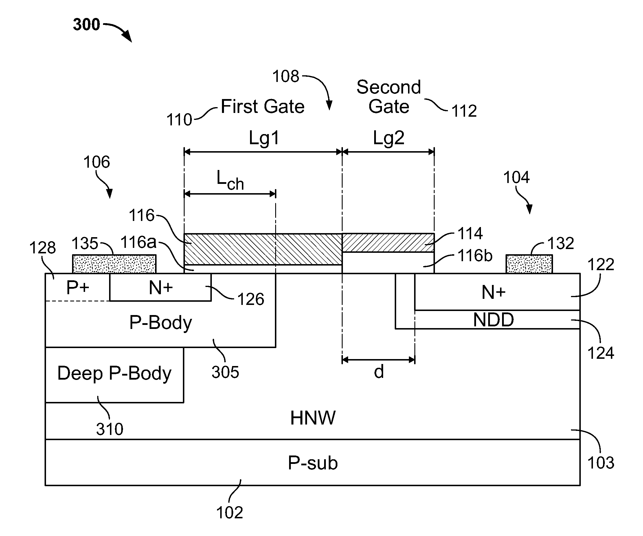
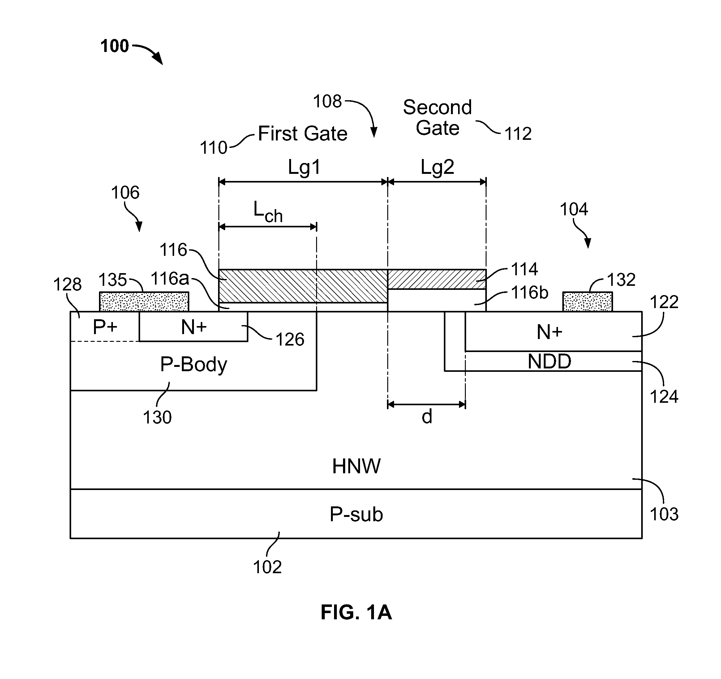
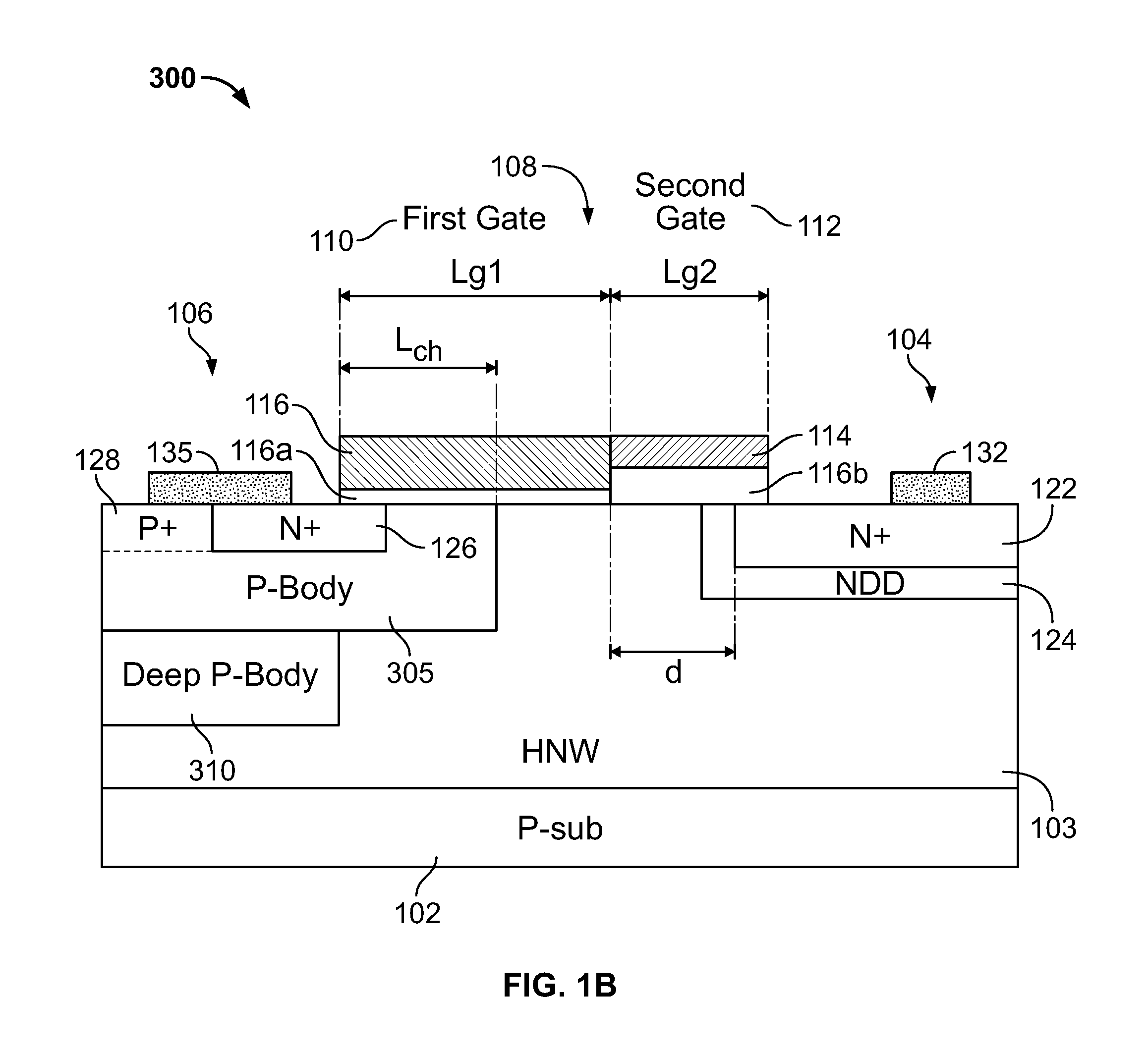
Capacitive losses degrade the efficiency of a transistor. One contribution to capacitance of the transistor is capacitance between the drain and source. Without being limited to any particular theory, capacitance between the drain and source of a transistor is a function of the gradient of the voltage potential between the drain and source. By providing the transistor with a doping profile that spreads the voltage potential gradient between the drain and source, i.e., by lowering the gradient by spreading the voltage potential difference across a larger volume, it is possible to have a transistor that exhibits lower capacitive losses.

Another contribution to the capacitance of the transistor is capacitance between the gate and drain. Without being limited to any particular theory, capacitance between the gate and drain is a function of the gradient of the voltage potential between the gate electrode and drain. The capacitive losses can also be reduced by having a dual gate including ...


PUM


Abstract

A transistor includes an n-well implanted in a substrate, a source region including a p-body region, a n+ region and a p+ region in the p-body region, a drain region comprising a n+ region, and a gate between the source region and the drain region. The p-body region includes a first implant region having a first depth, a first lateral spread and a first concentration of a p-type impurity, and a second implant region having a second depth, a second lateral spread and a second concentration of the p-type impurity. The second depth is less than the first depth, the second lateral spread is greater than the first lateral spread and the second concentration is greater than the first concentration. The p+ region and n+ region abut the second implant region.

Description

TECHNICAL FIELDThe following disclosure relates to semiconductor devices, and more particularly to a lateral diffused MOSFET (LDMOS) device.BACKGROUNDVoltage regulators, such as DC to DC converters, are used to provide stable voltage sources for electronic systems. Efficient DC to DC converters are particularly needed for battery management in low power devices, such as laptop notebooks and cellular phones. Switching voltage regulators (or simply “switching regulators”) are known to be an efficient type of DC to DC converter. A switching regulator generates an output voltage by converting an input DC voltage into a high frequency voltage, and filtering the high frequency input voltage to generate the output DC voltage. Specifically, the switching regulator includes a switch for alternately coupling and decoupling an input DC voltage source, such as a battery, to a load, such as an integrated circuit. An output filter, typically including an inductor and a capacitor, is coupled betwe...

Claims


Application Information

Patent Timeline
Patent Type & Authority Applications(United States)
IPC IPC(8): H01L29/78H01L21/336
CPCH01L29/0878H01L29/1095H01L29/7816H01L29/42368H01L29/66681H01L29/402
Inventor ZUNIGA, MARCO A.
Owner VOLTERRA SEMICONDUCTOR
Why Eureka
Try Eureka