
Diamond electrode and method for manufacturing diamond electrode

Inactive Publication Date: 2011-10-13
KURITA WATER INDUSTRIES LTD +1
View PDF3 Cites 18 Cited by
  • Summary
  • Abstract
  • Description
  • Claims
  • Application Information

AI Technical Summary

Benefits of technology

[0038]According to the present invention, it is possible to obtain a nonporous surface of a diamond film by increasing the thickness of a diamond film to a predetermined value or more. It is, thus, possible to prevent the deterioration of an electrode by the separation of a diamond film. The present invention is especially effective for a diamond-covered electrode including a diamond film covering at least one surface of a substrate.
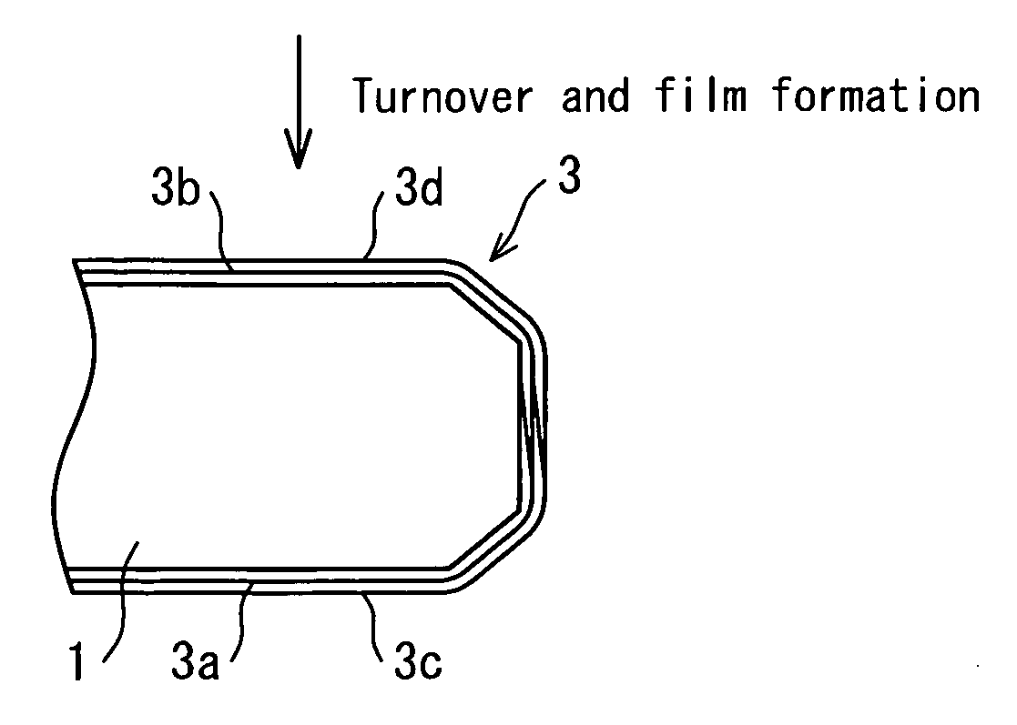
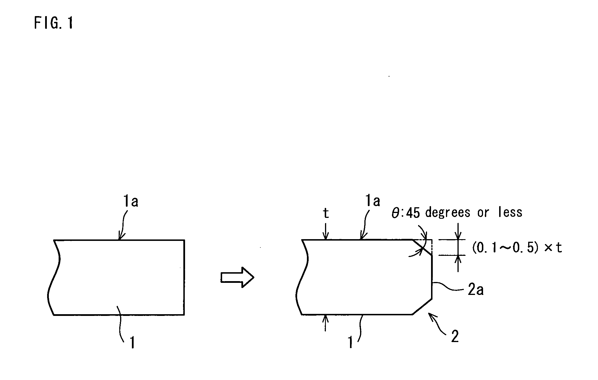
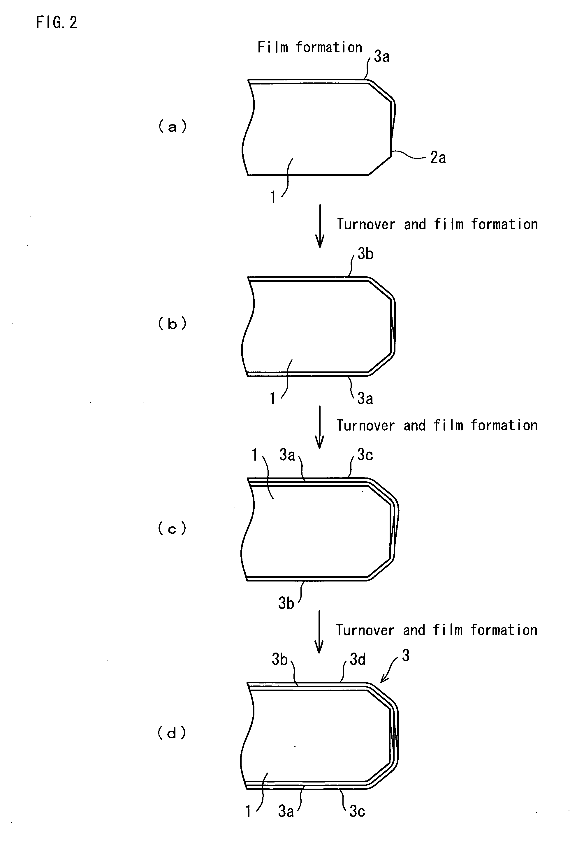
[0039]In a diamond-covered electrode of the present invention, predetermined chamfering is applied to edge parts of a substrate, and a diamond film with a thickness of a predetermined value or more is formed even on edge surfaces of the substrate too. It is, thus, possible to realize the excellent fixation between a substrate and diamond even at the edge parts of the substrate, and prevent the deterioration by the concentration of electric field on the edge parts. It is, therefore, possible to manufacture a diamond electrode able to prevent the deterioration of an electrode by the separation of a diamond film

Problems solved by technology

In the field of diamond electrodes, however, a problem remains that seeds cannot be generated well in a deep part of a recessed region.
It is, however, difficult to obtain nonporous diamond film.
In addition, if crack generates in a diamond film, the metal substrate elutes into electrolysis solution.
Electrode deterioration is, thus, caused.
From such a probability, it will be especially risky to adopt an electrode covered with diamond depositing on a metal substrate in a system for supplying cleaning solution for electronic materials such as semiconductor wafers.
Non-Patent Document 1, however, describes that the endurance of a diamond electrode is insufficient by such as separation of an electrically conductive diamond film formed on a silicon substrate.
In addition, since electric field concentrates on edge parts of an electrode, the edge parts are fragile and most likely to encounter separation.

Method used


Image

  • Diamond electrode and method for manufacturing diamond electrode
  • Diamond electrode and method for manufacturing diamond electrode
  • Diamond electrode and method for manufacturing diamond electrode

Examples


example 1

[0076]Next, examples of the present invention and reference examples are described, but the present invention is not limited to the examples.

examples 1-3

, Reference example 1

Difference in Thickness of Diamond Layer, Electrolysis of High-Concentration Sulfuric Acid

[0077]Electrically conductive silicon substrates (12 cm square and 3 mm thick) each having a volume resistivity of 0.5 ohm-cm were used. Edge parts of each substrate were subjected to the chamfering having a size of a width of 0.3 mm and an angle of 45 degrees. Surfaces of each substrate were adjusted to the maximum height of 1 μm and average roughness of 0.5 μm. After cleaning the entire surfaces of each substrate, first, diamond powder was seeded and then film forming was started. Hot filament CVD method was adopted for the film formation: a process pressure was 4 kPa, hydrogen, methane and trimethyl borate were used as introduced gases. The mixing volume ratio of hydrogen and methane was 100:2 and a small amount of trimethyl borate was added to the mixture. During the formation of a diamond layer, boron of 5,000 ppm with respect to carbon content was doped to provide ele...

example 4 , example 5

Example 4, Example 5

Difference in Thickness of Diamond Film, Electrolysis of Low-Temperature High-Concentration Sulfuric Acid

[0080]Under the same condition as example 1 and example 2 except a temperature of sulfuric acid solution to be electrolyzed at 30° C., the temperature being a severer electrolysis condition, sulfuric acid solution was similarly electrolyzed as above. The operation was continued at a current density of 30 A / dm2 for 200 hours.

[0081]As to an electrolysis cell using diamond electrodes with the thickness of a diamond film of 20 μm (example 4), in contrast with no deterioration after 200 hours in the above example 1, the electrolysis voltage during operation became unstable after about 150 hours in this example under the temperature of sulfuric acid solution at 30° C. as shown in Table 2. After the electrolysis, the electrolysis cell was disassembled and surfaces of the electrodes were examined to find that about 5% of the diamond film of the electrodes separated fr...


PUM

PropertyMeasurementUnit
Temperatureaaaaaaaaaa
Fractionaaaaaaaaaa
Thicknessaaaaaaaaaa

Abstract

A diamond electrode having an oxidation resistant diamond film which will not separate from the electrode during electrolysis with highly oxidizing materials. The thickness of the diamond film is 20 pm or more and the diamond film should preferably cover opposite side surfaces of a substrate in such a manner as to also cover end surfaces 2a of the substrate. The surfaces of the substrate are covered with a plurality of diamond layers to form the film using repeated steps of forming separate diamond layers with each diamond layer having a thickness of 10 to 30 pm on one of the surfaces of the substrate and then forming a diamond layer having a thickness of 10 to 30 pm on the other surface of the substrate. Thus, it is possible to form a nonporous surface of diamond layer and prevent deterioration of an electrode caused by the separation of a diamond film.

Description

TECHNICAL FIELD[0001]The present invention relates to a diamond electrode and a manufacturing method therefor, and especially to an oxidation resistant diamond electrode formed by covering surfaces of an electrically conductive substrate such as silicon with a diamond film and used especially for the electrolysis of highly oxidizing electrolysis solution.BACKGROUND ART[0002]Known methods for forming film of gas-phase synthesized diamond include microwave plasma CVD, hot filament CVD and DC arc jet plasma CVD. Diamond obtained by these methods normally exhibits electrical insulation, but electrically conductive diamond provided with electrical conductivity can be manufactured by adding impurity during the formation of film.[0003]Since diamond is a chemically very stable substance and excellent in the endurance against oxidation, the above-mentioned electrically conductive diamond attracts attention as an electrode especially used for water treatment and electrolysis.[0004]Important t...

Claims


Application Information

Patent Timeline
IPC IPC(8): C25B11/12B05D5/12H01B5/00
CPCC02F1/46109C23C16/271C25B11/0447C02F2001/46138C25B11/075C25B1/28C25B11/043
Inventor NAGAI, TATSUOIKEMIYA, NORIHITOYOSHIDA, KATSUHITOYOSHIDA, SHIGERU
Owner KURITA WATER INDUSTRIES LTD
Learn More