Structured pillar electrodes

a technology of pillar electrodes and electrodes, applied in the field of structured electrodes, can solve the problems of uncompetitive si-based pv power production with conventional fossil fuel-based energy sources, complex and expensive fabrication processes, and low material and manufacturing costs, and achieve the effect of higher power conversion efficiency gains

Inactive Publication Date: 2011-10-13
BROOKHAVEN SCI ASSOCS
View PDF1 Cites 64 Cited by
  • Summary
  • Abstract
  • Description
  • Claims
  • Application Information

AI Technical Summary

Benefits of technology

[0011]Having recognized the above and other considerations, the inventors determined that there is a continuing need to develop structures which address the inefficiencies associated with charge generation and transport in photovoltaic devices. In particular, there is a need for photovoltaic devices with significantly higher power conversion efficiency gains than have been realized to date. In view of the above-described problems, needs, and

Problems solved by technology

Despite the continued progression of Si thin film PV cells, their material and manufacturing costs remain relatively high, making Si-based PV power production uncompetitive with conventional fossil fuel-based energy sources.
Contributing factors include the need for large Si film thicknesses for efficient light absorption (≧200 μm), as well as their complex and expensive (requiring both time and energy) fabrication processes.
However, planar organic heterojunctions are generally inefficient as a photo-active layer since the diffusion length of generated bound electron-hole pairs (i.e., excitons), which later dissociate into f

Method used


Image

  • Structured pillar electrodes
  • Structured pillar electrodes
  • Structured pillar electrodes

Examples


Embodiment Construction

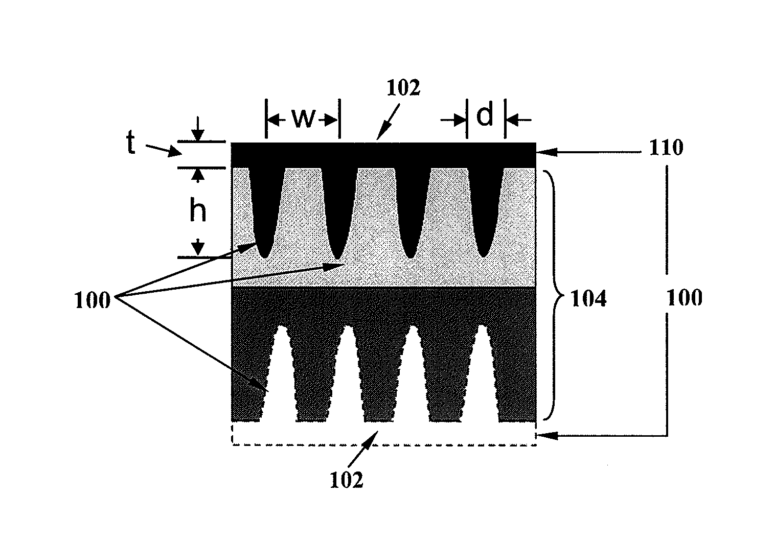
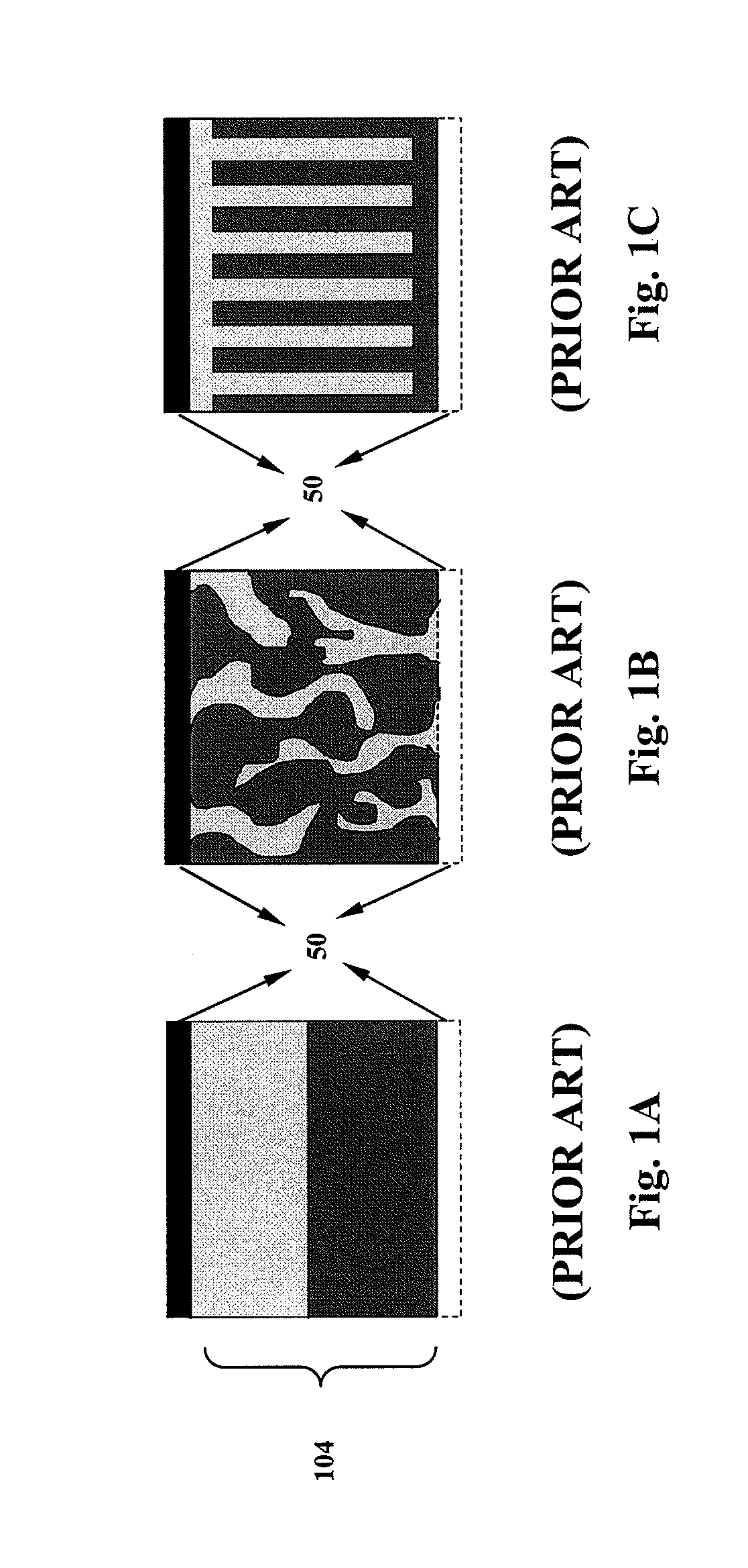
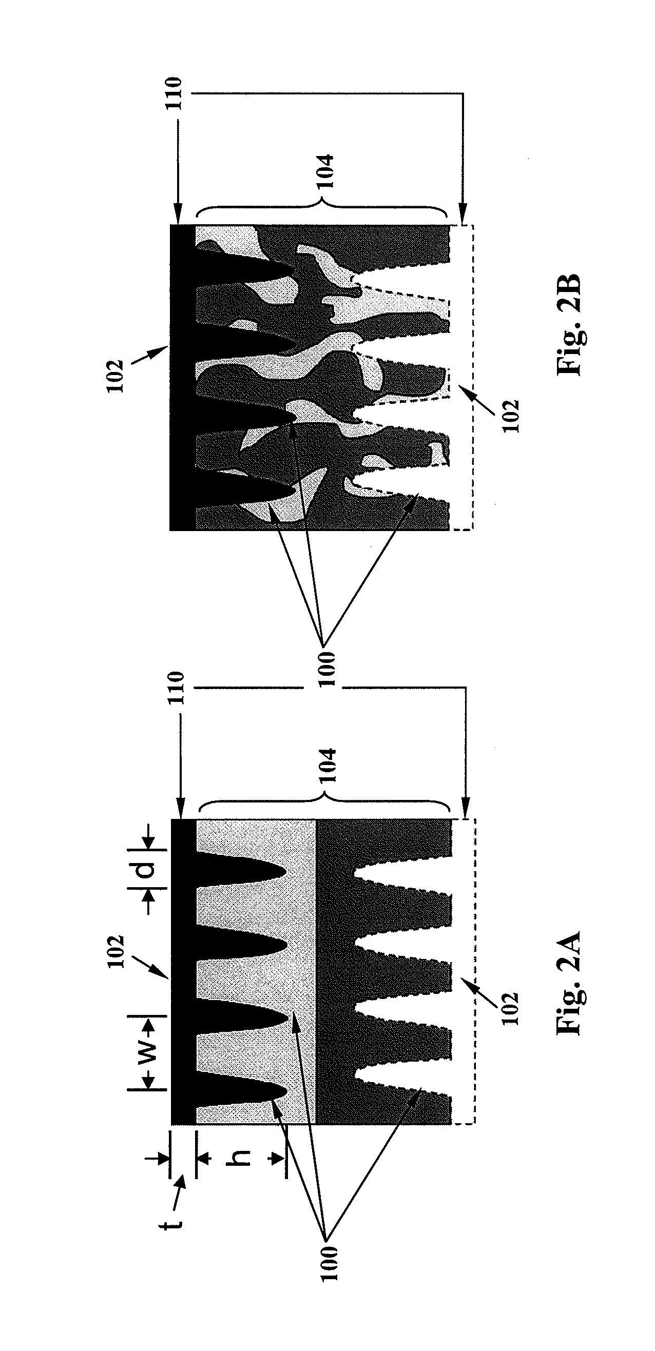
[0028]The above and other objectives of the invention will become more apparent from the following description and illustrative embodiments which are described in detail with reference to the accompanying drawings. Similar elements in each Figure are designated by like reference numbers and, hence, subsequent detailed descriptions thereof may be omitted for brevity. In the interest of clarity, in describing the embodiments of the present invention, the following terms and acronyms are defined as provided below.

Acronyms

[0029]CVD: Chemical Vapor Deposition[0030]ITO: Indium Tin Oxide[0031]LED: Light Emitting Diode[0032]FTO: Fluorinated Tin Oxide[0033]MBE: Molecular Beam Epitaxy[0034]PEDOT:PSS: poly(3,4-ethylenedioxythiophen:poly(styrene sulfanate))[0035]PCE: Power Conversion Efficiency[0036]PV: Photovoltaic[0037]PVD: Physical Vapor Deposition[0038]RIE: Reactive Ion Etching

Definitions

[0039]Acceptor: A dopant atom which, when added to an inorganic semiconductor, can form p-type regions...


PUM

PropertyMeasurementUnit
Fractionaaaaaaaaaa
Pore sizeaaaaaaaaaa
Pore sizeaaaaaaaaaa

Abstract

An electrode comprising a plurality of structured pillars dispersed across a base contact and its method of manufacture are described. In one embodiment the structured pillars are columnar structures having a circular cross-section and are dispersed across the base surface as a uniformly spaced two-dimensional array. The height, diameter, and separation of the structured pillars are preferably on the nanometer scale and, hence, electrodes comprising the pillars are identified as nanostructured pillar electrodes. The nanostructured pillars may be formed, for example, by deposition into or etching through a surface template using standard lithography processes. Structured pillar electrodes offer a number of advantages when incorporated into optoelectronic devices such as photovoltaic cells. These include improved charge collection efficiency via a reduction in the carrier transport distance and an increase in electrode-photoactive layer interface surface area. These improvements contribute to an increase in the power conversion efficiency of photovoltaic devices.

Description

CROSS-REFERENCE TO RELATED APPLICATIONS[0001]This application claims priority to U.S. Provisional Patent Application No. 61 / 088,826 which was filed on Aug. 14, 2008 and is incorporated by reference as if fully set forth in this specification.STATEMENT OF GOVERNMENT LICENSE RIGHTS[0002]The present invention was made with government support under Grant No. DE-AC02-98CH10886 awarded by the U.S. Department of Energy, Division of Chemical and Material Sciences. The United States government has certain rights in the invention.BACKGROUND OF THE INVENTION[0003]I. Field of the Invention[0004]This invention relates generally to structured electrodes. In particular, the present invention relates to electrodes having vertically aligned pillars dispersed across a horizontal base contact. The invention also relates to the manufacture of such structured pillar electrodes and their use in electronic devices such as solar cells.[0005]II. Background of the Related Art[0006]A photovoltaic cell is an e...

Claims


Application Information

Patent Timeline
IPC IPC(8): H01L31/0336H01L31/18
CPCB82Y10/00H01L31/022425H01L31/022466Y02E10/549H01L51/0036H01L51/0047H01L51/4253H01L31/1884H10K85/113H10K85/215H10K30/30H10K30/50
Inventor NAM, CHANG-YONGBLACK, CHARLES T.GEARBA, IOANA R.ALLEN, JONATHAN EDWARD
Owner BROOKHAVEN SCI ASSOCS
Why Eureka
Try Eureka