Semiconductor device structure and method for manufacturing the same

a technology of semiconductor devices and semiconductor electrodes, applied in the direction of semiconductor devices, electrical devices, nanotechnology, etc., can solve the problems of increasing leakage current and power consumption, increasing the depletion effect of polysilicon electrodes, and increasing the eot of devices, so as to reduce the eot effect of devices

Inactive Publication Date: 2011-10-20
INST OF MICROELECTRONICS CHINESE ACAD OF SCI
View PDF2 Cites 18 Cited by
  • Summary
  • Abstract
  • Description
  • Claims
  • Application Information

AI Technical Summary

Benefits of technology

[0006]The present invention aims to at least solve one of the abovementioned technical defects, and particularly, to bring forth effects of reducing EOT of the devices without negative impact on the high k dielectrics layer by introducing “an indirect oxygen absorption process”.
[0010]In the present invention, a metal gate oxygen absorbing layer is introduced into the metal gate for the purpose of preventing the outside oxygen from coming into the interface layer and absorbing the oxygen in the interface layer during the annealing process, such that the interface layer is reduced to be thinner and the EOT of MOS devices are effectively reduced. Meanwhile, ascribing to adding an oxygen absorption element barrier layer, the “oxygen absorption element” is prevented from diffusing into the high k gate dielectric layer and giving rise to unfavorable impact thereon. In this way, the high k / metal gate system can be more easily integrated, and the performance of the device can be further improved accordingly.

Problems solved by technology

However, with continued scaling of the feature size, the SiO2 gate dielectric within MOS transistor almost come to its limit.
With further scaling, the leakage current and power consumption may increase dramatically.
Meanwhile, the problems such as diffusion of doped boron atoms, polysilicon depletion effect and overly high gate resistance arising from polysilicon electrode will be increasingly aggravated.
However, the high-temperature annealing process has to be applied in the high k / metal gate process, which, as a result, would make the SiO2 interface layer become thicker during the annealing process.
On the other hand, the CMOS devices at the 45 nm node and below need gate dielectrics with EOT (Equivalent Oxide Thickness) no thicker than 1 nm to improve the gate control of the channel, which the relatively thick SiO2 interface layer is impossible to fulfill.
Accordingly, how to reduce EOT, particularly to reduce EOT attributed by the SiO2 interface layer, becomes a critical challenge for the new generation of high k / metal gate technology.
In short, during a high-temperature thermal process, the oxygen within the interface layer is driven to form metallic oxide(s) with “such a metal or unsaturated oxidized dielectric that absorbs oxygen”, which thus reduces the thickness of the interface layer, and even makes it depleted.
Nonetheless, such a “direct oxygen absorption process” that introduces “an oxygen absorption metal” into high k gate dielectric is still subject to some shortcomings, for instance, such kind of “oxygen absorption metal” would directly result in the change of the high k gate dielectric, and give rise to other unfavorable impacts on the performance of MOS devices.

Method used


Image

  • Semiconductor device structure and method for manufacturing the same
  • Semiconductor device structure and method for manufacturing the same
  • Semiconductor device structure and method for manufacturing the same

Examples


Embodiment Construction

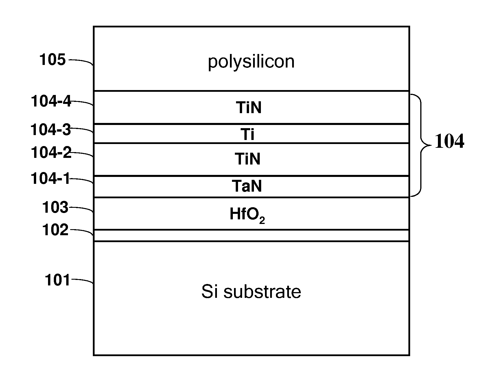
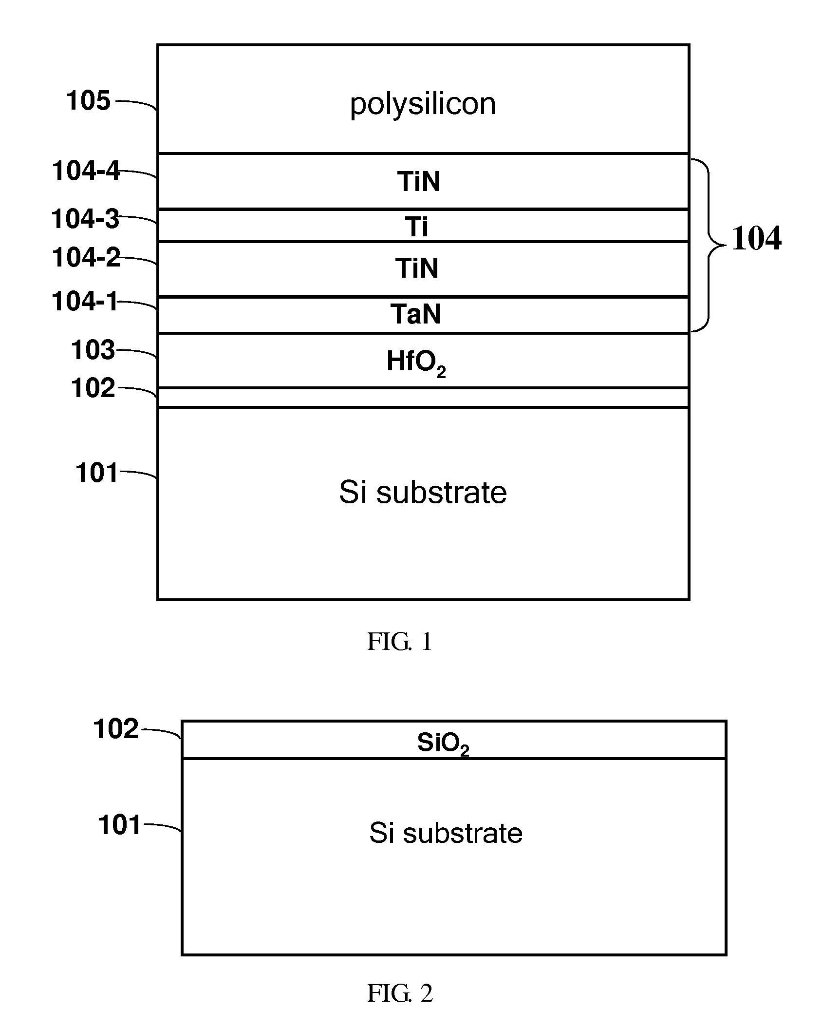
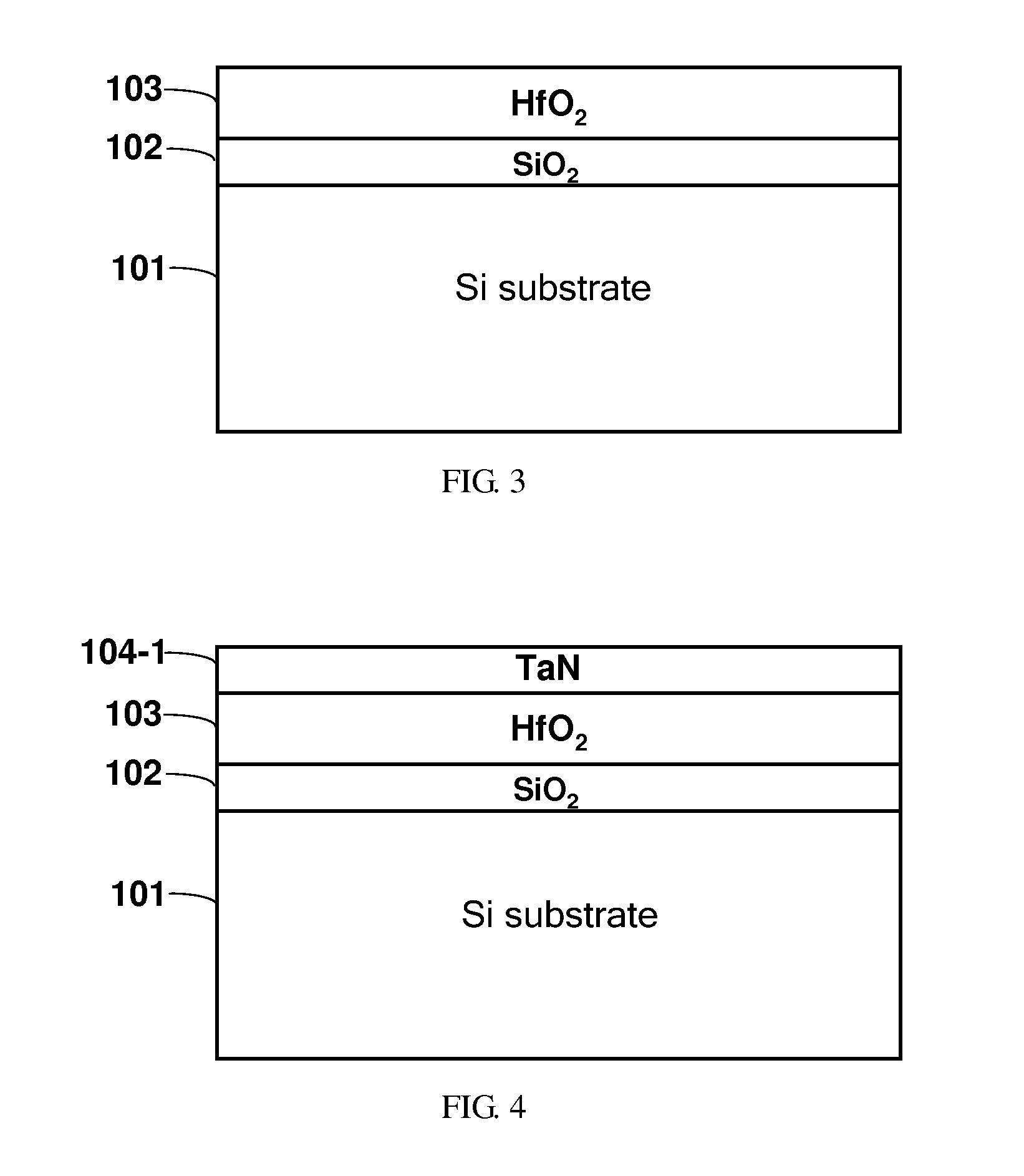
[0015]Described below in detail are the embodiments of the present invention, whose exemplary models also are illustrated in the drawings; wherein the same or similar numbers throughout the drawings denote the same or similar elements or elements have the same or similar functions. The embodiments described below with reference to the drawings are merely illustrative, and are provided for explaining the present invention only, thus should not be interpreted as a limit to the present invention.

[0016]The following disclosure provides a plurality of different embodiments or examples to achieve different structures of the present invention. To simplify the disclosure of the present invention, description of the components and arrangements of specific examples is given below. Of course, they are only illustrative and not limiting the present invention. Moreover, in the present invention, reference numbers and / or letters may be repeated in different embodiments. Such repetition is for the...


PUM

PropertyMeasurementUnit
thicknessaaaaaaaaaa
thicknessaaaaaaaaaa
thicknessaaaaaaaaaa

Abstract

The present invention provides a MOS device, which comprises: a substrate; an interface layer thin film formed on the substrate; a high k gate dielectric layer formed on the interface layer thin film; and a metal gate formed on the high k gate dielectric layer. The metal gate comprises, upwardly in order, a metal gate work function layer, an oxygen absorption element barrier layer, a metal gate oxygen absorbing layer, a metal gate barrier layer and a polysilicon layer. A metal gate oxygen absorbing layer is introduced into the metal gate for the purpose of preventing the outside oxygen from coming into the interface layer and absorbing the oxygen in the interface layer during a annealing process, such that the interface layer is reduced to be thinner and the EOT of MOS devices are effectively reduced; meanwhile, by adding an oxygen absorption element barrier layer, the “oxygen absorption element” is prevented from diffusing into the high k gate dielectric layer and giving rise to unfavorable impact thereon; in this way, the high k / metal gate system can be more easily integrated, and the performance of the device can be further improved accordingly.

Description

FIELD OF THE INVENTION[0001]The present invention relates to design and fabrication of semiconductor, and particularly, to a semiconductor structure and a method for manufacturing the same.BACKGROUND OF THE INVENTION[0002]In the past decades which witnessed the development of the microelectronics technology, logic chip manufacturers always made use of SiO2 as gate dielectric and heavily doped polysilicon as the gate electrode when manufacturing MOS devices. However, with continued scaling of the feature size, the SiO2 gate dielectric within MOS transistor almost come to its limit. For example, in the 65 nm process, the thickness of the SiO2 gate dielectric is lowered to 1.2 nm, which namely is equivalent of the thickness of about 5 silicon atom layers. With further scaling, the leakage current and power consumption may increase dramatically. Meanwhile, the problems such as diffusion of doped boron atoms, polysilicon depletion effect and overly high gate resistance arising from polys...

Claims


Application Information

Patent Timeline
Patent Type & Authority Applications(United States)
IPC IPC(8): H01L29/78H01L21/321B82Y40/00B82Y99/00
CPCH01L21/28088H01L29/42372H01L29/517H01L29/513H01L29/4966
Inventor CHEN, SHIJIEWANG, WENWUWANG, XIAOLEIHAN, KAI
Owner INST OF MICROELECTRONICS CHINESE ACAD OF SCI
Why Eureka
Try Eureka