Method of manufacturing semiconductor apparatus

a manufacturing method and semiconductor technology, applied in the direction of electrical equipment, semiconductor devices, semiconductor/solid-state device details, etc., can solve the problems of short life of the semiconductor apparatus or the lower reliability of the semiconductor apparatus, the reduced throughput of non-defective semiconductor apparatus products, and the reduced warp of the semiconductor chip. , the effect of reducing the warp of the semiconductor chip

Active Publication Date: 2011-10-20
FUJI ELECTRIC CO LTD
View PDF0 Cites 31 Cited by
  • Summary
  • Abstract
  • Description
  • Claims
  • Application Information

AI Technical Summary

Benefits of technology

[0087]According to the invention, a tape is stuck to the back surface of a semiconductor wafer in the step of sticking such that the bending state of the semiconductor wafer, in which the semiconductor wafer is bending convexly toward the front surface side, is maintained. Since the step of plating is conducted in the bending state, in which the semiconductor wafer is bending convexly toward the front surface side, the tensile stresses on the front and back surface sides of the semiconductor wafer balance to each other. Therefore, the semiconductor wafer is brought into an almost flat state, after the tape is removed. Therefore, the warp of the semiconductor chip cut out from the semiconductor wafer is reduced. Since the warp of the semiconductor chip is reduced, it is possible to absorb the semiconductor chip exactly at the right position on a stage in measuring the electric characteristics of the semiconductor chip and to measure the electric characteristics of the semiconductor chip securely.
[0088]Since the warp of the semiconductor chip is reduced, the voids due to the warp of the semiconductor chip are prevented from occurring in the solder layer in the step of mounting the semiconductor chip. Therefore, the mounting position deviation of the semiconductor chip and the short-circuit fault caused by the voids in the solder layer are prevented from occurring. The life of the semiconductor apparatus is prevented from becoming shorter.
[0089]Since the warp of the semiconductor chip is reduced, the entire or a part of the solder layer is prevented from becoming thinner than the predetermined thickness in mounting the semiconductor chip. Therefore, the mounting position deviation of the semiconductor chip and the short-circuit fault caused by the nonuniform solder layer thickness are prevented from occurring. The life of the semiconductor apparatus is prevented from becoming shorter.
[0090]In the step of sticking, the entire back surface electrode is covered with a film or a tape (hereinafter referred to simply as a “tape,” and in the claims as a “first film”). By conducting the step of plasma treatment before the step of sticking, the adhesive strength between the back surface electrode and the tape is improved. Therefore, the back surface electrode is protected securely with the tape. As the back surface electrode is protected securely with the tape, the plating solution never comes in between the back surface electrode and the tape in the step of plating. Since the back surface electrode surface is not exposed to the plating solution, the wettability of the back surface electrode to a solder is prevented from being impaired. Therefore, voids are prevented from occurring in the boundary between the back surface electrode and the solder layer in bonding the semiconductor chip manufactured by cutting the semiconductor wafer into chips with a solder.
[0091]By the manufacturing method according to the invention, the reliability of the semiconductor apparatus is improved. By the manufacturing method according to the invention, the semiconductor apparatuses are manufactured with a high throughput of non-defective products. By the manufacturing method according to the invention, external appearance anomalies are prevented from occurring on the back surface electrode.

Problems solved by technology

As the results of the researches explored vigorously by the present inventors, it has been found that the problems as described below will be caused, if a semiconductor chip is manufactured by any of the techniques disclosed by Japanese Patent Publication No. 3829860 and Japanese Unexamined Patent Application Publication No. 2009-054965.
Therefore, the throughput of non-defective semiconductor apparatus products will be impaired.
Or else, the entire solder layer or a part of the solder layer is thinned due to the warp tC of semiconductor chip 101, resulting in the short life of the semiconductor apparatus or the lower reliability of the semiconductor apparatus.
Further, semiconductor chip 101 or the metal plate may be displaced from the right bonding position or a short-circuit fault may be caused due to the warp tC of semiconductor chip 101, resulting in the low throughput of non-defective semiconductor apparatus products.
If the back surface electrode is exposed to the plating solution, the plating material will segregate abnormally on the back surface electrode, the edge portion surface of the surface electrode will be tarnished (hereinafter referred to as “external appearance anomalies”), and such a new problem will be caused.
If external appearance anomalies are caused on the back surface electrode, the wettability of the back surface electrode to the solder will be impaired.
If the wettability of the back surface electrode to the solder is not good, voids will be caused in the boundary between the back surface electrode and the solder layer in mounting the semiconductor device by bonding with a solder.
The voids caused will lower the reliability of the semiconductor apparatus.

Method used


Image

  • Method of manufacturing semiconductor apparatus
  • Method of manufacturing semiconductor apparatus
  • Method of manufacturing semiconductor apparatus

Examples


first embodiment

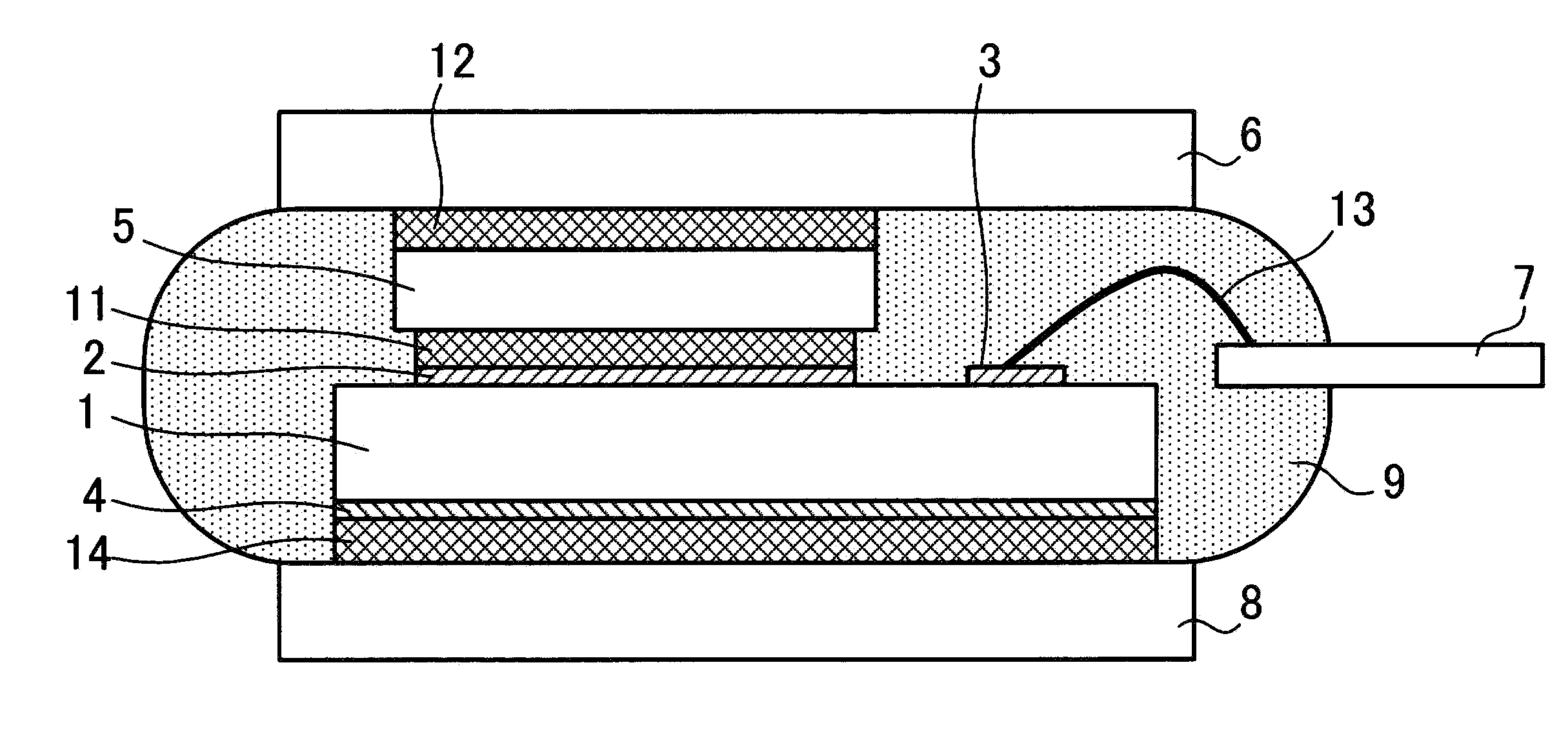
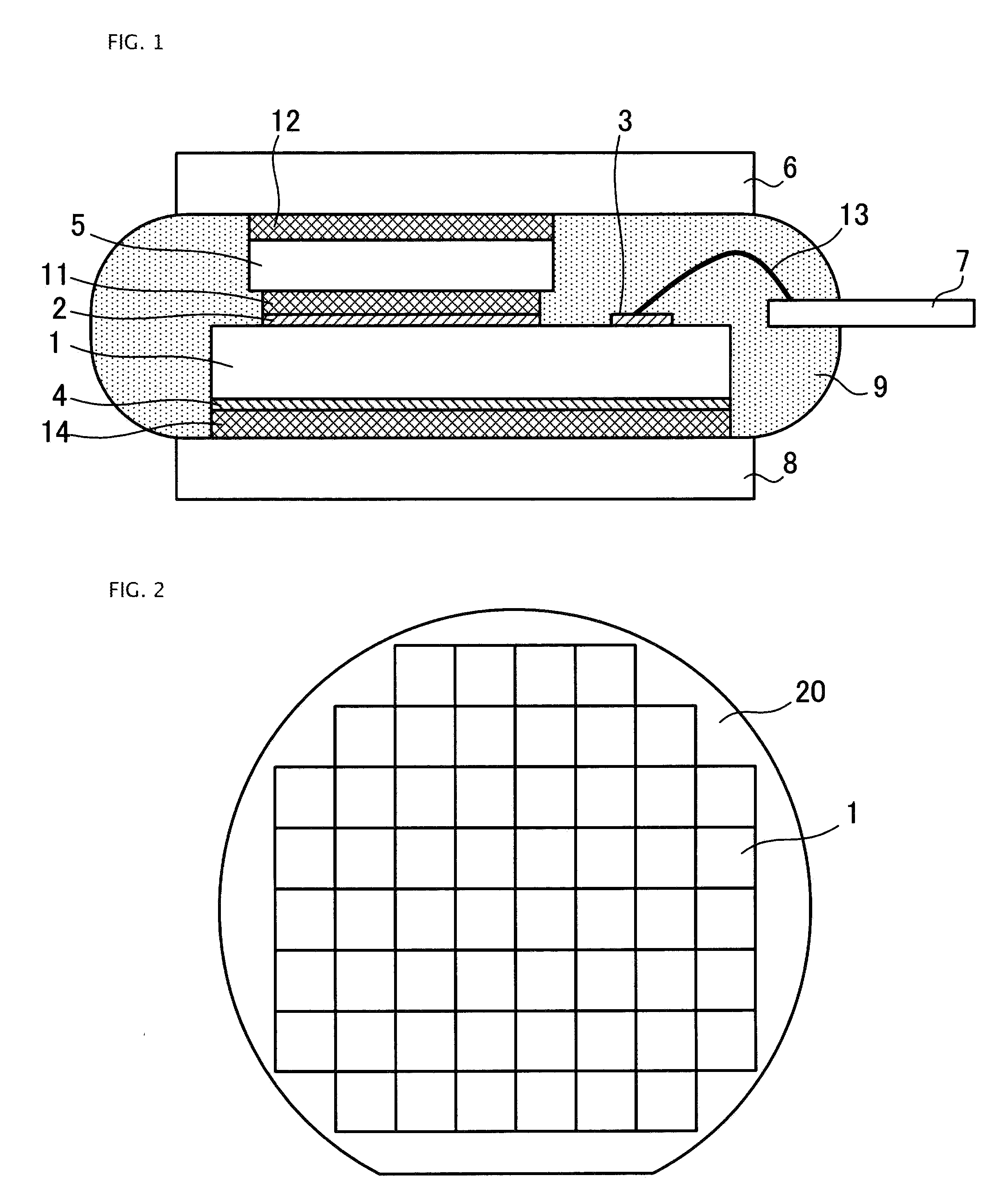
[0118]FIG. 1 is a cross sectional view of a semiconductor apparatus according to a first embodiment of the invention. In FIG. 1, the front surface structure is not shown.

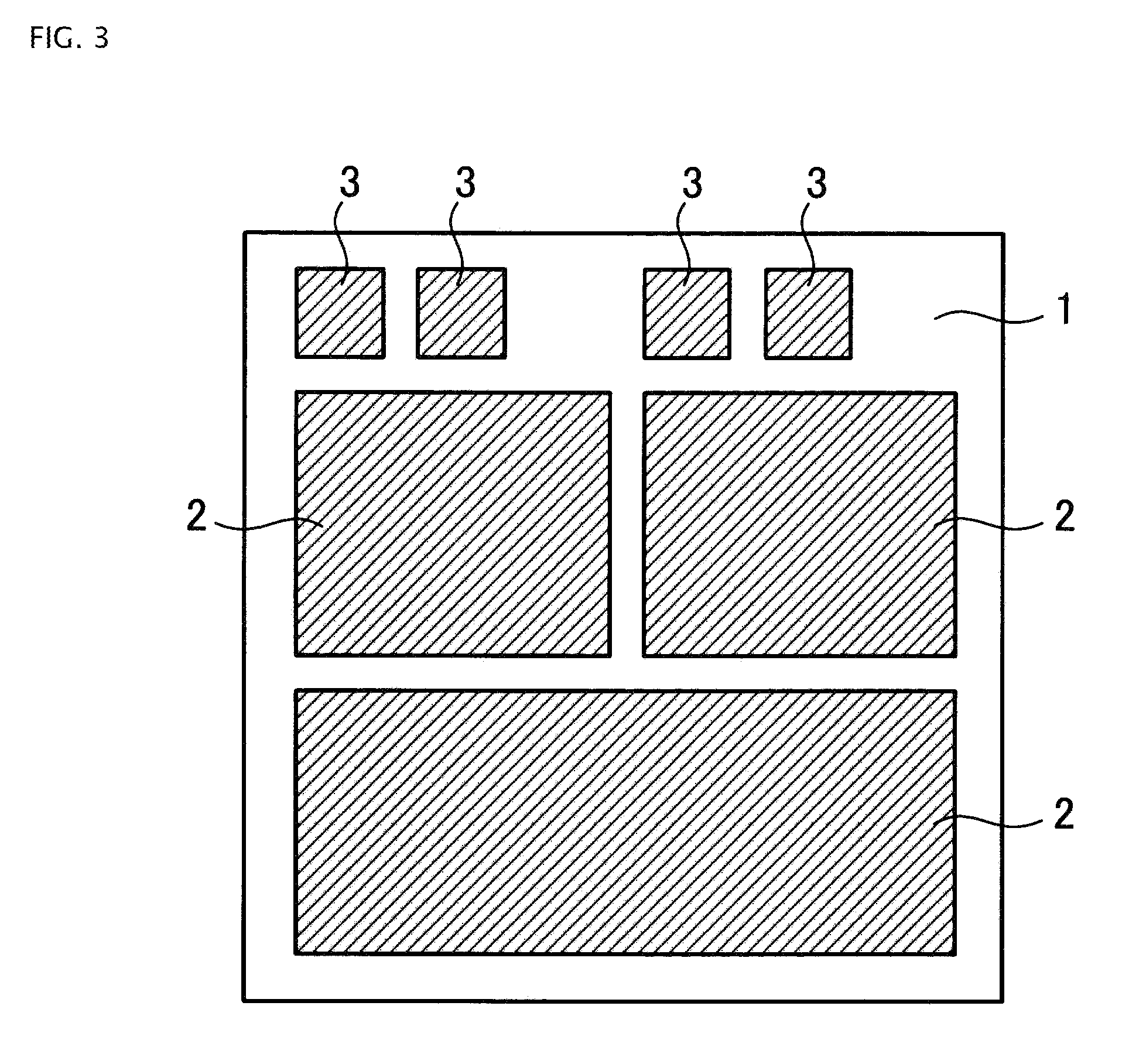
[0119]Referring now to FIG. 1, first front surface electrode 2 functioning as an emitter electrode and second front surface electrode 3 functioning as a gate electrode are formed on the front surface of semiconductor chip 1. A semiconductor device such as an IGBT (not shown) is formed in semiconductor chip 1. First front surface electrode 2 is formed of an emitter electrode and a plate film covering the emitter electrode. Back surface electrode 4 is formed on the back surface of semiconductor chip 1. Back surface electrode 4 is a collector electrode, for example.

[0120]First front surface electrode 2 is bonded to metal plate 5 via solder layer 11. Metal plate 6 is bonded via solder layer 12 to metal plate 5 surface opposite to metal plate 5 surface, to which first front surface electrode 2 is bonded. Second front sur...

second embodiment

[0171]It is also effective to stick removable adhesive tape 23 to the back surface of semiconductor wafer 20 to intentionally make semiconductor wafer 20 bend convexly toward the front surface side.

[0172]According to the second embodiment, removable adhesive tape 23 is stuck to make semiconductor wafer 20 bend more convexly toward the front surface side in the step of sticking than the bending state of semiconductor wafer 20 in the step of forming a back surface electrode. For example, it is effective to heat removable adhesive tape 23 or to exert a tensile stress to removable adhesive tape 23 in the same manner as according to the first embodiment.

[0173]According to the second embodiment, the step of plating is conducted after making semiconductor wafer 20 bend further convexly toward the front surface side as described above. If the bending state caused only by back surface electrode 4 is maintained in the same manner as according to the first embodiment, the tensile stress caused...

third embodiment

[0176]FIG. 16 is a schematic describing a plasma treatment apparatus according to a third embodiment of the invention. As shown in FIG. 16, plasma treatment apparatus 30 includes a capacitively coupled plasma generation mechanism, formed of a pair of flat electrodes 31 and 32, between which semiconductor wafers 20 are placed. Electrode 31 is connected to the ground. Electrode 32 is connected to a high-frequency power source 33. The pair of electrodes 31 and 32 functions as a capacitor. Quartz boat 34 that supports a plurality of semiconductor wafers 20 is between electrodes 31 and 32.

[0177]Quartz boat 34 includes four rod-shaped supporting parts that support the semiconductor wafers 20 edges on the electrode 31 side and plate-shaped connecting parts (not shown) connected to the end portions of the supporting parts. The supporting parts are placed in parallel to the surfaces of electrodes 31 and 32. The supporting parts include grooves as wide as to hold the edge portion of semicondu...


PUM


Abstract

A method of manufacturing a semiconductor apparatus includes forming back surface electrode 4 on back surface of semiconductor wafer 20, that bends convexly toward the front surface side due to back surface electrode 4 being formed; treating the back surface with a plasma for removing the deposits on the back surface; sticking removable adhesive tape 23 to the back surface along the warp thereof for maintaining the bending state of semiconductor wafer 20 after the step of sticking; electrolessly plating to form film 26 on the front surface of semiconductor wafer 20; peeling off removable adhesive tape 23; cutting out semiconductor chips; and mounting the semiconductor chip by bonding with a solder for manufacturing a semiconductor apparatus. The manufacturing method prevents external appearance anomalies from occurring on the back surface electrode, improves the reliability, and allows manufacture of the semiconductor apparatuses with a high throughput of non-defective products.

Description

BACKGROUND OF THE INVENTION[0001]A. Field of the Invention[0002]The present invention relates to a method of manufacturing a semiconductor apparatus.[0003]B. Description of the Related Art[0004]An insulated gate bipolar transistor (hereinafter referred to as an “IGBT”), that is one of the power semiconductor devices, exhibits high-speed switching performances and voltage-driven characteristics, which the metal-oxide-semiconductor field-effect transistor (hereinafter referred to as a “MOSFET”) exhibits, and low ON-state voltage characteristics, which the bipolar transistor exhibits. The IGBT's expand the application fields thereof from general-purpose inverters, AC servos, uninterruptible power sources (UPS's), and switching power supplies to boost DC-DC converters for hybrid vehicles.[0005]For manufacturing the semiconductor devices described above, a method described below is proposed in Japanese Unexamined Patent Application Publication No. 2007-036211. A surface structure is form...

Claims


Application Information

Patent Timeline
Patent Type & Authority Applications(United States)
IPC IPC(8): H01L21/50H01L21/28
CPCH01L21/6836H01L23/3107H01L24/03H01L24/05H01L24/06H01L24/29H01L24/32H01L24/45H01L24/48H01L24/73H01L2221/68372H01L2221/68386H01L2224/03464H01L2224/0381H01L2224/04026H01L2224/04042H01L2224/05571H01L2224/05644H01L2224/06181H01L2224/29111H01L2224/32245H01L2224/45124H01L2224/45144H01L2224/48247H01L2224/73215H01L2224/741H01L2224/93H01L2924/01013H01L2924/01029H01L2924/0103H01L2924/01033H01L2924/01079H01L2924/01082H01L2924/014H01L2924/09701H01L2924/13055H01L2924/13091H01L2924/3511H01L2224/48699H01L2924/01005H01L2924/01006H01L2924/01043H01L2924/01047H01L2924/0105H01L2924/01074H01L2924/0132H01L2924/0133H01L2224/73265H01L2924/15747H01L2224/48644H01L2924/01014H01L2924/01028H01L2924/10253H01L2224/05553H01L2224/05554H01L2224/0603H01L2924/1306H01L2924/1305H01L2224/48091H01L2924/0002H01L2224/03H01L2924/01015H01L2924/00012H01L2924/00014H01L2924/00H01L2224/48744H01L2224/05552H01L2924/181H01L2224/2612
Inventor URANO, YUICHI
Owner FUJI ELECTRIC CO LTD
Why Eureka
Try Eureka