Method for Synthesis of High Quality Large Area Bulk Gallium Based Crystals

a gallium based crystal and large area technology, applied in the direction of crystal growth process, polycrystalline material growth, chemically reactive gas, etc., can solve the problems of thermal expansion mismatch, impurities, tilt boundaries, and additional defects, etc., to achieve the effect of reducing the number of defects, and reducing the quality of the devi

Active Publication Date: 2011-10-20
SLT TECH
View PDF2 Cites 87 Cited by
  • Summary
  • Abstract
  • Description
  • Claims
  • Application Information

AI Technical Summary

Benefits of technology

[0010]In an alternative specific embodiment, the present invention provides a method for forming a gallium based crystal, which may be used for other applications. The method includes providing a laterally grown gallium based seed crystal, which has a maximum length of at least 25 mm and a first thickness substantially orthogonal to a first direction of the maximum length and a second thickness orthogonal to the first direction of the maximum length. Each of the first thickness and the sec...

Problems solved by technology

The quality and reliability of these devices, however, is compromised by high defect levels, particularly threading dislocations, grain boundaries, and strain in semiconductor layers of the devices.
Additional defects can arise from thermal expansion mismatch, impurities, and tilt boundaries, depending on the details of the growth method of the layers.
The presence of defects has a deleterious effect on epitaxially-grown layers.
Such effect includes compromising electronic d...

Method used


Image

  • Method for Synthesis of High Quality Large Area Bulk Gallium Based Crystals
  • Method for Synthesis of High Quality Large Area Bulk Gallium Based Crystals
  • Method for Synthesis of High Quality Large Area Bulk Gallium Based Crystals

Examples


Embodiment Construction

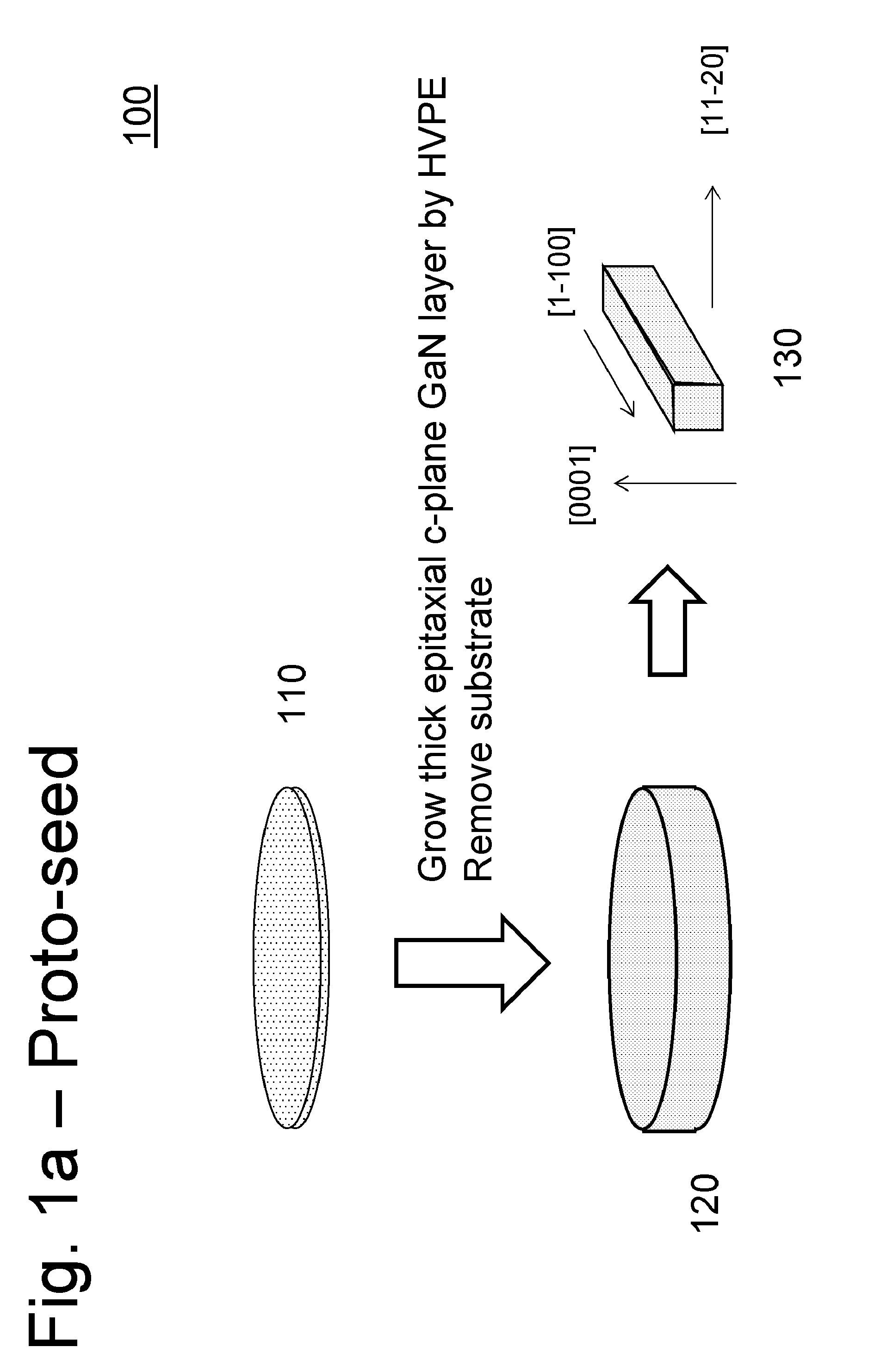
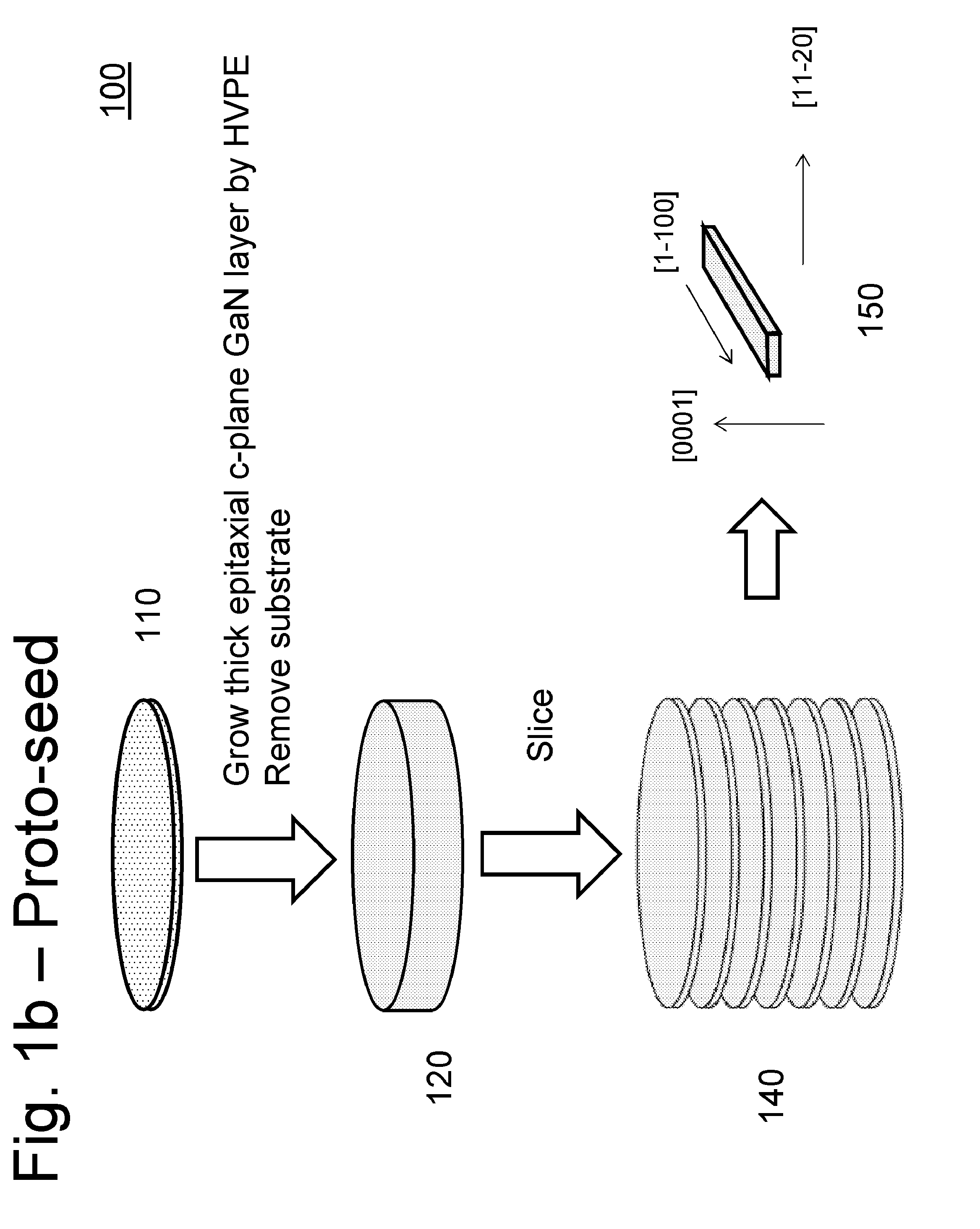
[0026]According to the present invention, techniques related to techniques for processing materials for manufacture of gallium based substrates are provided. More specifically, embodiments of the invention include techniques for growing large area substrates using a combination of processing techniques. Merely by way of example, the invention can be applied to growing crystals of GaN, AlN, InN, InGaN, AlGaN, and AlInGaN, and others for manufacture of bulk or patterned substrates. Such bulk or patterned substrates can be used for a variety of applications including optoelectronic devices, lasers, light emitting diodes, solar cells, photo electrochemical water splitting and hydrogen generation, photodetectors, integrated circuits, and transistors, and others.

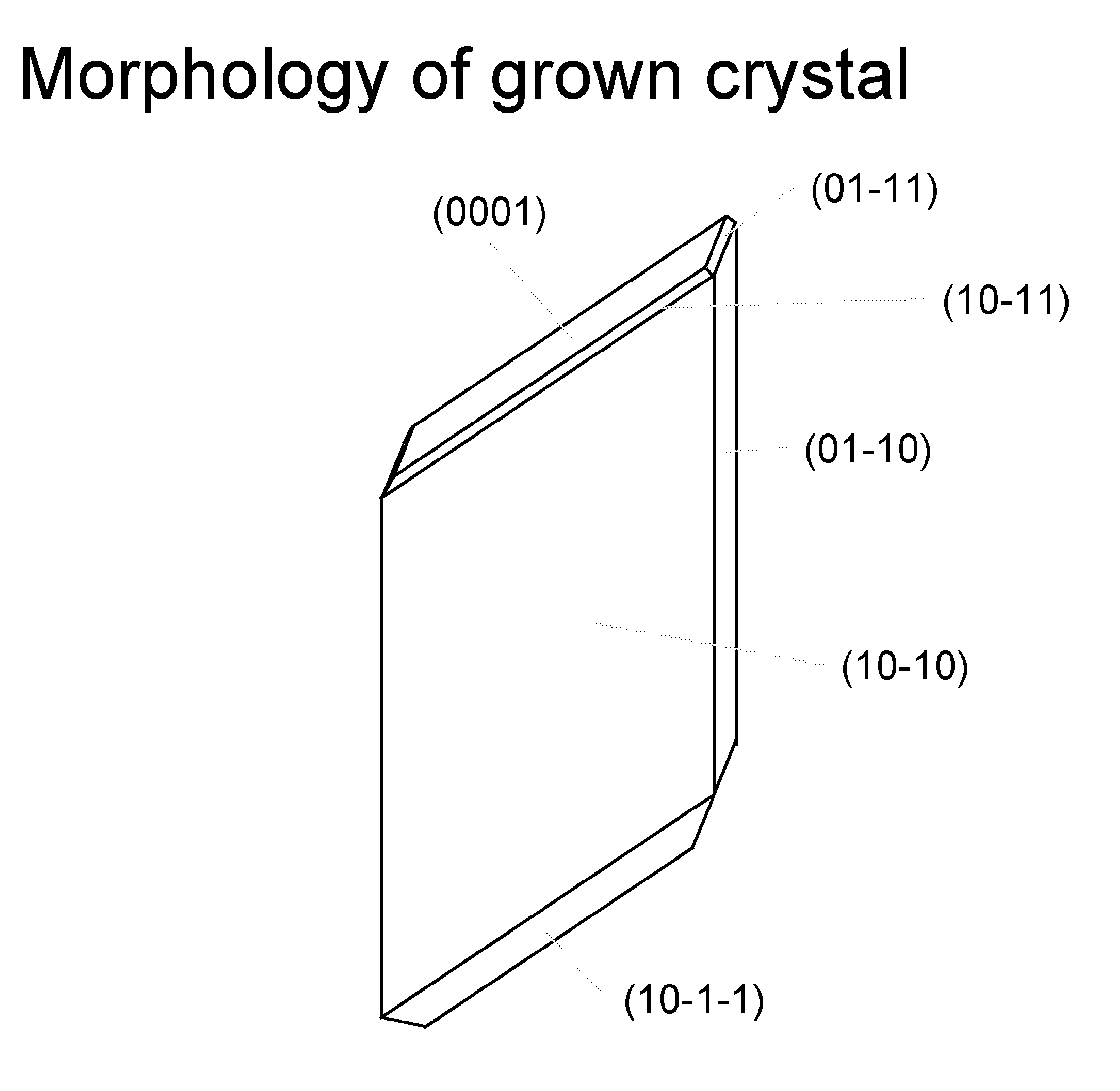
[0027]D'Evelyn and co-inventors, in U.S. Pat. No. 7,078,731, hereby incorporated by reference in its entirety, taught methods for growing gallium nitride crystals. We have found that these methods have some limitations. FIG. 5 in ...


PUM


Abstract

A large area nitride crystal, comprising gallium and nitrogen, with a non-polar or semi-polar large-area face, is disclosed, along with a method of manufacture. The crystal is useful as a substrate for a light emitting diode, a laser diode, a transistor, a photodetector, a solar cell, or for photoelectrochemical water splitting for hydrogen generation.

Description

CROSS-REFERENCE TO RELATED APPLICATION[0001]This application claims priority to U.S. Provisional No. 61 / 250,476, filed Oct. 9, 2009, commonly assigned, and hereby incorporated by reference herein.BACKGROUND OF THE INVENTION[0002]This invention relates generally to techniques for processing materials for manufacture of gallium based substrates. More specifically, embodiments of the invention include techniques for growing large area substrates using a combination of processing techniques. The invention can be applied to growing crystals of GaN, AlN, InN, InGaN, AlGaN, and AlInGaN, and others for manufacture of bulk or patterned substrates. Such bulk or patterned substrates can be used for a variety of applications including optoelectronic devices, lasers, light emitting diodes, solar cells, photo electrochemical water splitting and hydrogen generation, photo detectors, integrated circuits, and transistors, and others.[0003]Gallium nitride (GaN) based optoelectronic and electronic dev...

Claims


Application Information

Patent Timeline
IPC IPC(8): H01L21/20C01B21/06C01B21/072C30B11/14
CPCC30B7/105C30B29/406C30B29/403C30B25/02C30B7/005H01L21/0254H01L21/02609H01L21/02645H01L21/02647H01L29/045H01L29/2003H01L29/34H01L29/36
Inventor D`EVELYN, MARK P.SPECK, JAMES S.
Owner SLT TECH
Why Eureka
Try Eureka