Silicon nitride films and methods

a technology of silicon nitride and film, applied in the direction of coating, metallic material coating process, chemical vapor deposition coating, etc., can solve the problems of unwanted carbon content in the film, occurrence and/or buildup of amine salts in the reaction chamber, and aforementioned finer feature is jeopardized, so as to reduce the carbon content of the film and reduce the effect of carbon conten

Inactive Publication Date: 2011-10-20
NOVELLUS SYSTEMS
View PDF6 Cites 617 Cited by
  • Summary
  • Abstract
  • Description
  • Claims
  • Application Information

AI Technical Summary

Benefits of technology

[0012]In some embodiments, the SiN film produced has an undesirable carbon content. This in-film carbon may result in electrical leakage and may render the film unusable for some dielectric barrier applications. Methods described herein produce SiN films with less than 2% carbon, in one embodiment less than 1% carbon, in yet another embodiment less than 0.5% carbon. In some embodiments, the reduction in carbon residue is readily observable in FTIR spectra. One embodiment is a method of forming a silicon nitride material on a substrate, including: (a) forming a silicon nitride film on the substrate, said formation including: (i) providing the substrate in a reaction chamber; (ii) exposing the substrate to a silicon-containing reactant in the vapor phase so that the silicon-containing reactant is adsorbed onto the surface of the substrate; (iii) exposing the substrate to an nitrogen-containing reactant in the vapor phase so that the nitrogen-containing reactant is adsorbed onto the surface of the substrate; (iv) igniting a plasma while the nitrogen-containing reactant is present in the vapor phase; and then, (b) exposing the silicon nitride film to a hydrogen containing plasma. The hydrogen plasma reduces carbon content of the film. In one embodiment, the hydrogen plasma is generated using hydrogen (H2) and a carrier gas such as nitrogen, helium or a

Problems solved by technology

One issue with SiN films is the relatively high temperatures used to form the films, for example, in Front End of Line (FEOL) applications, SiN films are typically deposited by chemical vapor deposition (CVD) in a reactor at greater than 750° C. using dichlorosilane and ammonia.
Another issue with SiN film depositions is the occurrence and/or buildup of amine salts in the reaction chamber.
Another issue with SiN films is, in certain instances, unwanted car

Method used


Image

  • Silicon nitride films and methods
  • Silicon nitride films and methods
  • Silicon nitride films and methods

Examples


example 1

[0117]Table 1 includes a number of reaction partners, and temperature and pressure parameters that may be used to make SiN films in accordance with the embodiments described herein.

TABLE 1Reactant AReactant BReactant CTemp(° C.)Press. (torr)Ref. indexBTBASNH3—50-5501-41.80-2.05BTBAS—N2 / H250-5501-41.80-2.05BTBASNH3N2 / H250-5501-41.80-2.05SiH3ClNH3Optionally50-5501-4N2 / H2SiH3ClTBAOptionallyN2 / H2SiH2Cl2NH3Optionally50-5501-41.80-2.05N2 / H2SiH2Cl2TBAOptionallyN2 / H2SiH(CH3)—(N(CH3)2)2NH3Optionally50-5501-41.80-2.05N2 / H2SiH(CH3)(Cl2)NH3Optionally50-5501-41.80-2.05N2 / H2SiHCl—(N(CH3)2)2NH3Optionally50-5501-41.80-2.05N2 / H2(Si(CH3)2NH)3NH3Optionally50-5501-41.80-2.05N2 / H2

example 2

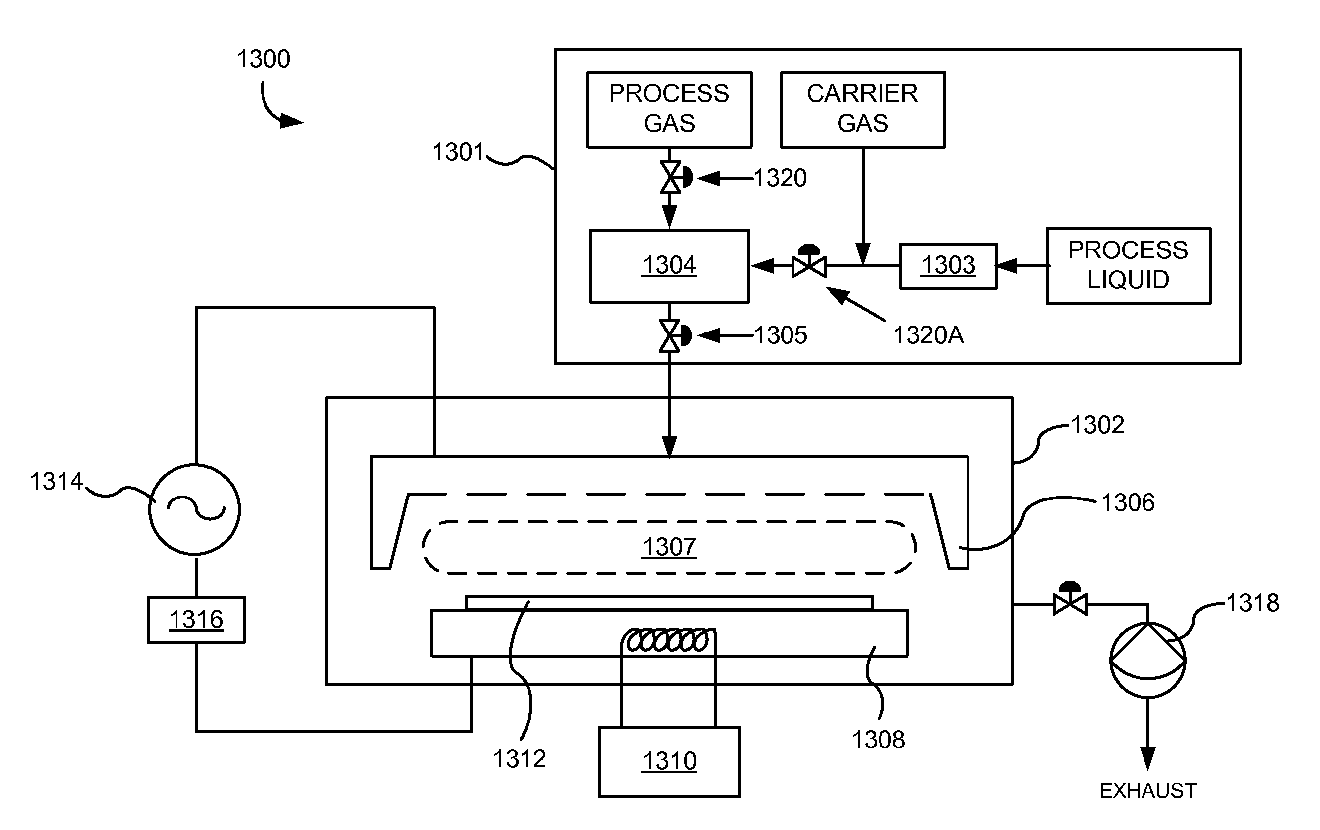
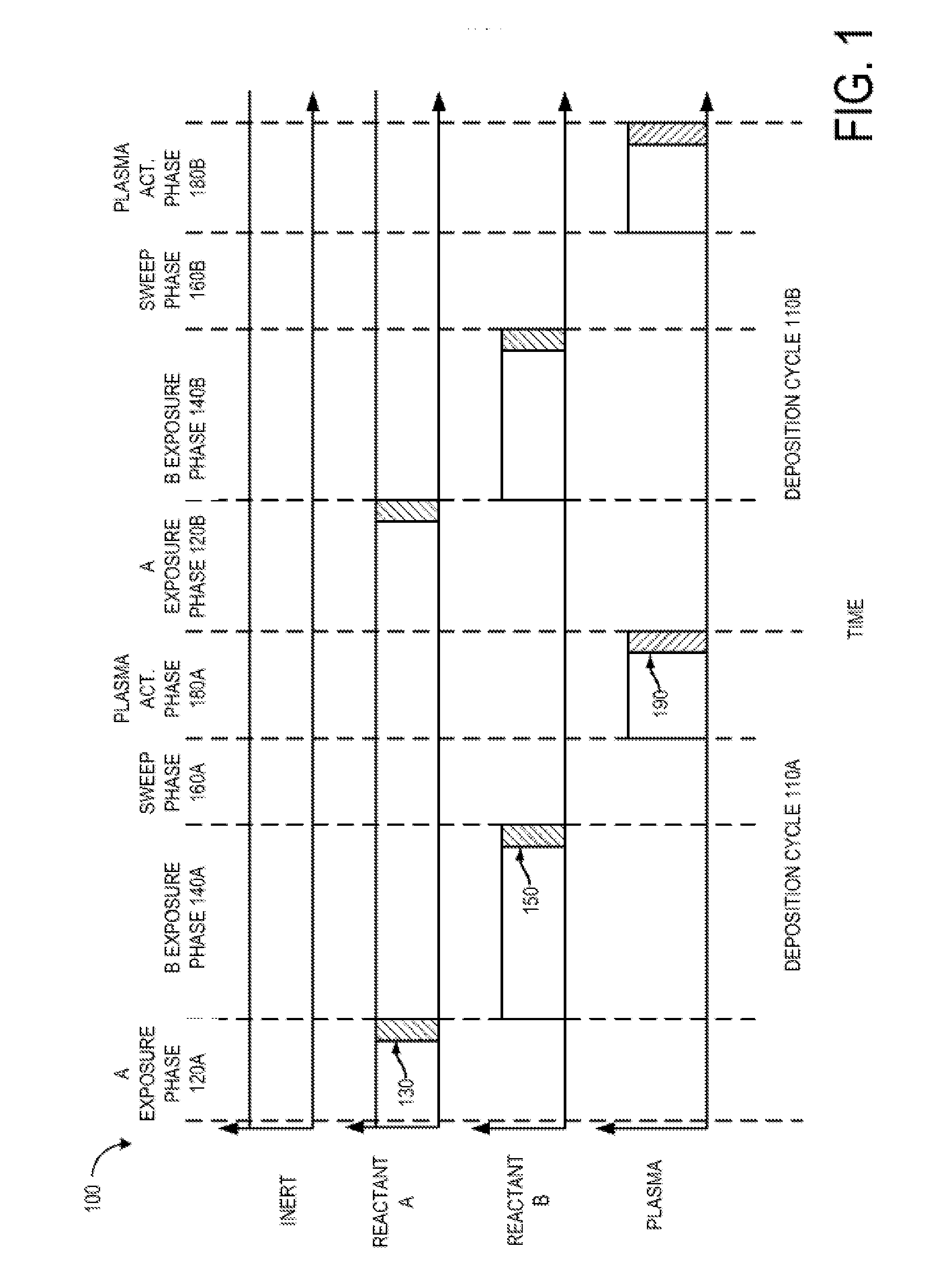
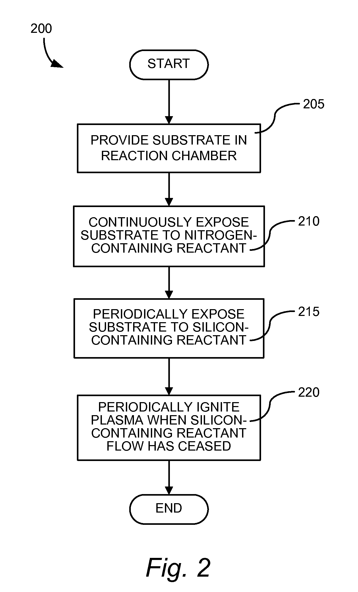
[0118]A 300 mm wafer is placed into vacuum chamber and the chamber evacuated to 0.5 torr. The wafer is supported within the chamber on an aluminum pedestal which is heated throughout the procedure. For example, the pedestal is heated at a constant temperature that is between about 50° C. and about 550° C. The pressure in the chamber is increased to 2 torr using an inert gas such as argon or nitrogen. Dichlorosilane (DCS) is introduced into the reactor as a vapor phase flow at between about 1 slm and about 5 slm (standard liters per minute) for between about 1 second and about 30 seconds in order to adsorb DCS onto the surface of the wafer. After the DCS flow is ceased, the inert gas flow in the reactor purges the remaining vapor phase DCS and any byproducts. Then, a t-butylamine (TBA) vapor phase flow is established in the reactor at between about 1 slm and about 5 slm for between about 1 second and about 30 seconds. A plasma, for example 13.56 MHz at 2.5 kW power, is ignited above ...


PUM

PropertyMeasurementUnit
Temperatureaaaaaaaaaa

Abstract

Described are methods of making SiN materials on substrates, particularly SiN thin films on semiconductor substrates. Improved SiN films made by the methods are also included.

Description

CROSS REFERENCE TO RELATED APPLICATIONS[0001]This application claims priority benefit under 35 USC §119(e) of U.S. provisional patent application No. 61 / 324,710, filed Apr. 15, 2010, and U.S. provisional patent application No. 61 / 372,367, filed Aug. 10, 2010, and U.S. provisional patent application No. 61 / 379,081, filed Sep. 1, 2010, and U.S. provisional patent application No. 61 / 417,807, filed Nov. 29, 2010, each of which is incorporated herein by reference in its entirety and for all purposes. This application is related to U.S. patent application Ser. No. ______ [Attorney docket No. NOVLP405], and U.S. patent application Ser. No. ______ [Attorney docket No. NVLS003674], each filed on the same day as the instant disclosure and each incorporated herein by reference in its entirety and for all purposes.INTRODUCTION[0002]1. Field[0003]The present disclosure relates generally to formation of SiN materials on substrates. More particularly, the disclosure relates to formation of SiN fil...

Claims


Application Information

Patent Timeline
IPC IPC(8): H01L21/318
CPCC23C16/045H01L21/76898C23C16/402C23C16/45523C23C16/4554C23C16/56H01L21/02164H01L21/0217H01L21/02274H01L21/0228H01L21/02348H01L21/28562H01L21/67017H01L21/6719H01L21/67201H01L21/76224H01L21/76825H01L21/76826H01L21/76829H01L21/76837C23C16/345C23C16/44C23C16/455H01L21/0262H01L21/3065
Inventor HAUSMANN, DENNIS M.HENRI, JONSRIRAM, MANDYAMVAN SCHRAVENDIJK, BART J.
Owner NOVELLUS SYSTEMS
Why Eureka
Try Eureka