

Silicon carbide substrate and method for manufacturing silicon carbide substrate
a technology of silicon carbide substrate and silicon carbide, which is applied in the direction of crystal growth process, polycrystalline material growth, after-treatment details, etc., can solve the problems of reducing the efficiency of semiconductor devices, reducing the size of sic single-crystal substrates, and reducing the efficiency of manufacturing semiconductor devices
- Summary
- Abstract
- Description
- Claims
- Application Information
AI Technical Summary
Benefits of technology
Problems solved by technology
Method used
Image

Examples
first embodiment
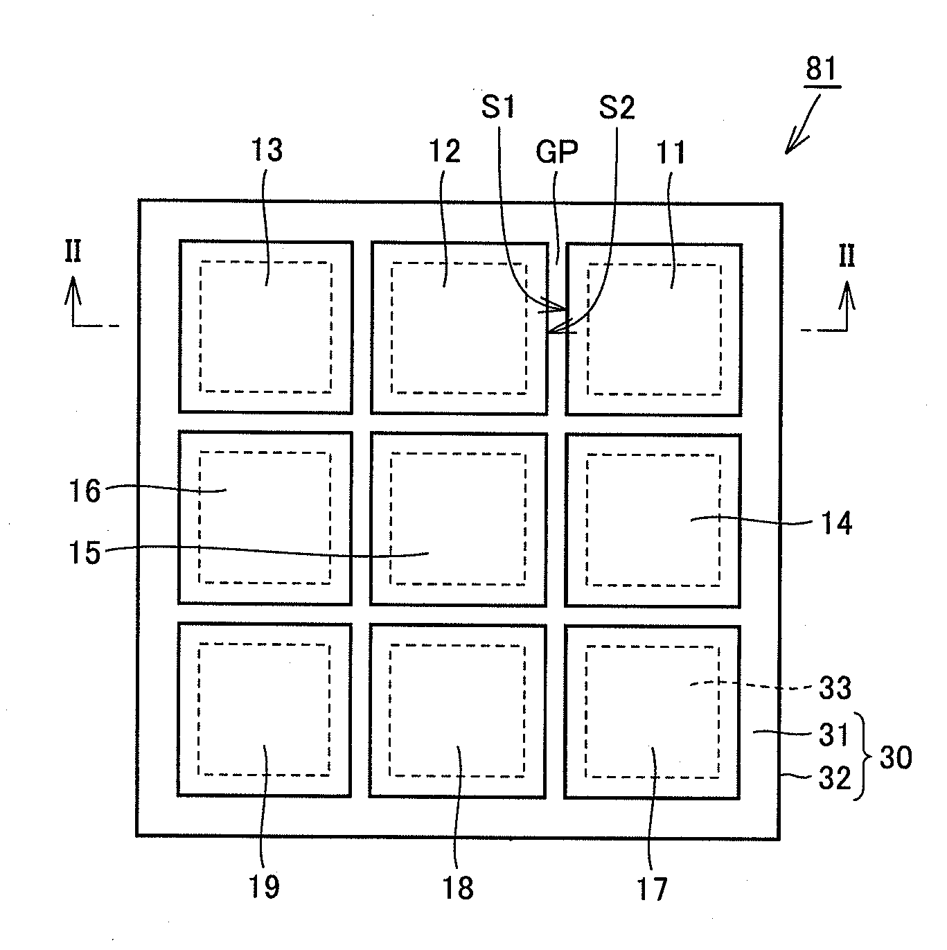
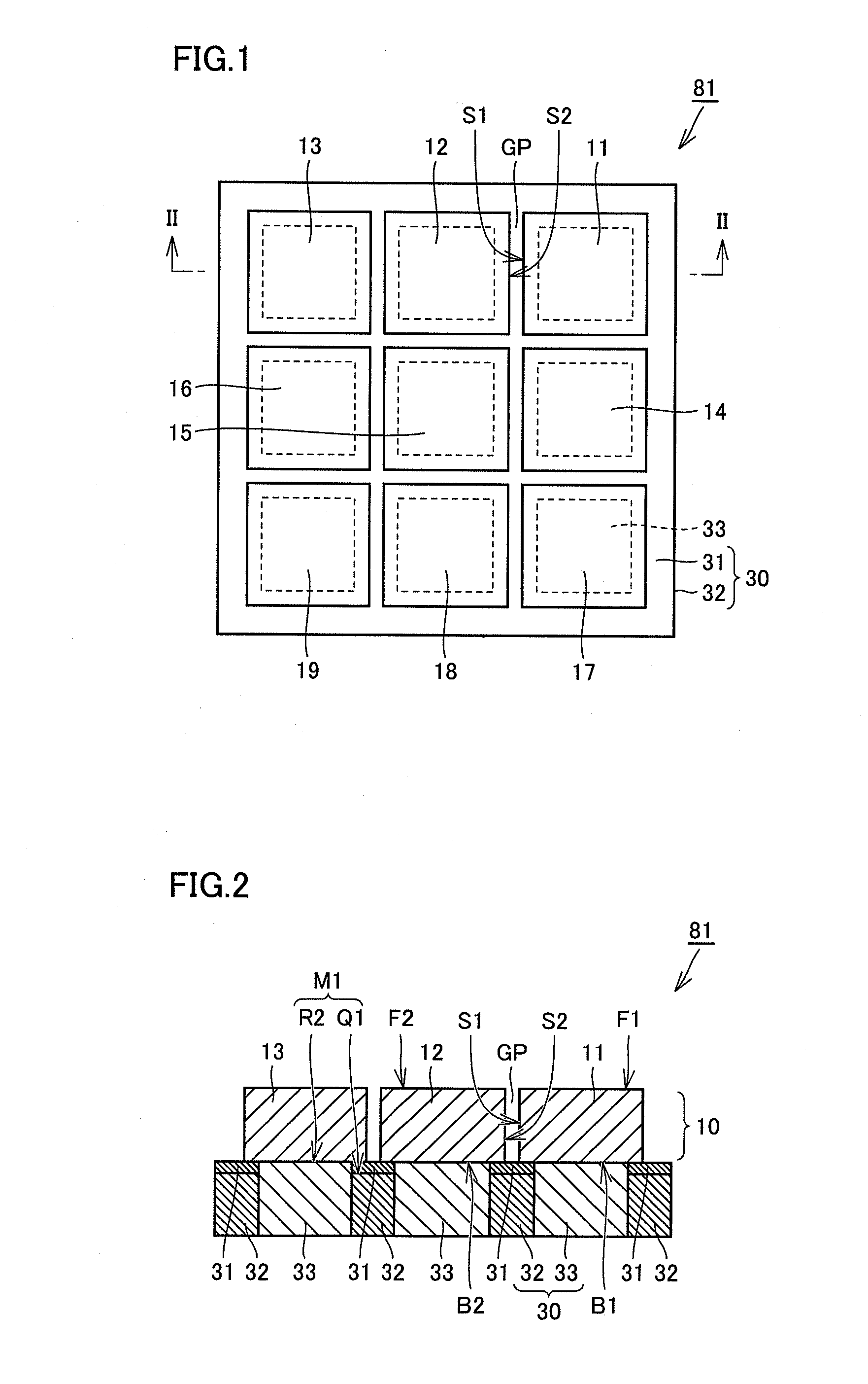
[0039]Referring to FIG. 1 and FIG. 2, a silicon carbide substrate 81 includes a base substrate 30, a carbon layer 31, and single-crystal layers 11-19 (also collectively referred to as “single-crystal layer 10”).
[0040]Base substrate 30 is made of silicon carbide, and has a non-growth portion 32 and regrowth portions 33. An interface between non-growth portion 32 and each regrowth portion 33 extends substantially in the direction of thickness (vertical direction in FIG. 2). Only regrowth portions 33 of non-growth portion 32 and regrowth portions 33 are portions formed by recrystallizing silicon carbide on single-crystal layer 10. Hence, only regrowth portions 33 of non-growth portion 32 and regrowth portions 33 are epitaxially grown under influence of the crystal structure of single-crystal layer 10. Accordingly, there is a crystallographic difference between non-growth portion 32 and each regrowth portion 33. Further, base substrate 30 has a main surface M1 (upper surface in FIG. 2) ...
second embodiment
[0064]Referring to FIG. 10, a silicon carbide substrate 82 of the present embodiment is different from silicon carbide substrate 81 of the first embodiment (FIG. 1) in that silicon carbide substrate 82 has a circular shape. Silicon carbide substrate 82 is obtained by cutting silicon carbide substrate 81 (FIG. 1) to have a circular shape. Preferably, the diameter of the circular shape is 5 cm or greater, more preferably, 15 cm or greater. Apart from the configuration described above, the configuration of the present embodiment is substantially the same as the configuration of the first embodiment. Hence, the same or corresponding elements are given the same reference characters and are not described repeatedly.
third embodiment
[0065]Referring to FIG. 11, a semiconductor device 100 of the present embodiment is a DiMOSFET (Double Implanted Metal Oxide Semiconductor Field Effect Transistor) of vertical type, and has regrowth portion 33, single-crystal layer 10, a buffer layer 121, a reverse breakdown voltage holding layer 122, p regions 123, n+ regions 124, p+ regions 125, an oxide film 126, source electrodes 111, upper source electrodes 127, a gate electrode 110, and a drain electrode 112. Semiconductor device 100 has a planar shape (shape when viewed from upward in FIG. 11) of, for example, a rectangle or a square with sides each having a length of 2 mm or greater.
[0066]Drain electrode 112 is provided on regrowth portion 33 and buffer layer 121 is provided on single-crystal layer 10. With this arrangement, a region in which flow of carriers is controlled by gate electrode 110 is disposed not in the regrowth portion 33 side but in the single-crystal layer 10 side. Each of regrowth portion 33 and single-crys...
PUM
| Property | Measurement | Unit |
|---|---|---|
| size | aaaaa | aaaaa |
| diameter | aaaaa | aaaaa |
| diameter | aaaaa | aaaaa |
Abstract
Description
Claims
Application Information