Multilayer ceramic capacitor, printed circuit board including the same, methods of manufacturing thereof

a multi-layer ceramic capacitor and printed circuit board technology, applied in the direction of variable capacitors, fixed capacitor details, printed circuit non-printed electric components association, etc., can solve problems such as defects and deterioration of characteristics, and achieve stable electrostatic capacitance and prevent cracking

Inactive Publication Date: 2011-11-03
SAMSUNG ELECTRO MECHANICS CO LTD
View PDF3 Cites 27 Cited by
  • Summary
  • Abstract
  • Description
  • Claims
  • Application Information

AI Technical Summary

Benefits of technology

[0009]An aspect of the present invention provides a multilayer ceramic capacitor capable of preventing cracking due to the diffusion of electrode materials while securing stable electrostatic capacitance, a printed circuit board including the same, a method of manufacturing the multilayer ceramic capacitor, and a method of manufacturing the printed circuit board.
[0015]According to another aspect of the present invention, there is provided a multilayer ceramic capacitor, including: a capacitor body, the capacitor body being dry polished such that surfaces of external electrodes thereof are smooth and compact; and plating layers formed on the surfaces of the external electrodes.

Problems solved by technology

An embedded chip, on which a surface treatment is not performed, may cause cracks, delamination, damage, or the like thereof, by laser erosion during a laser processing, thus leading to deteriorated characteristics and defects, such as shorts.

Method used


Image

  • Multilayer ceramic capacitor, printed circuit board including the same, methods of manufacturing thereof
  • Multilayer ceramic capacitor, printed circuit board including the same, methods of manufacturing thereof
  • Multilayer ceramic capacitor, printed circuit board including the same, methods of manufacturing thereof

Examples


example 1

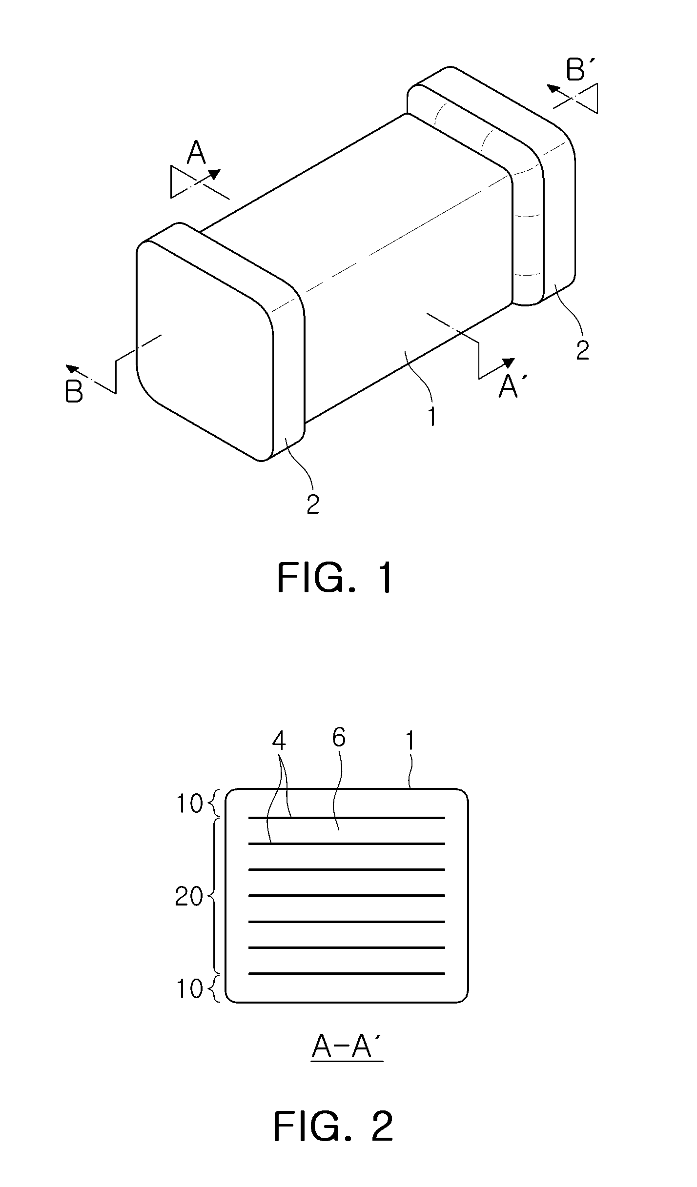
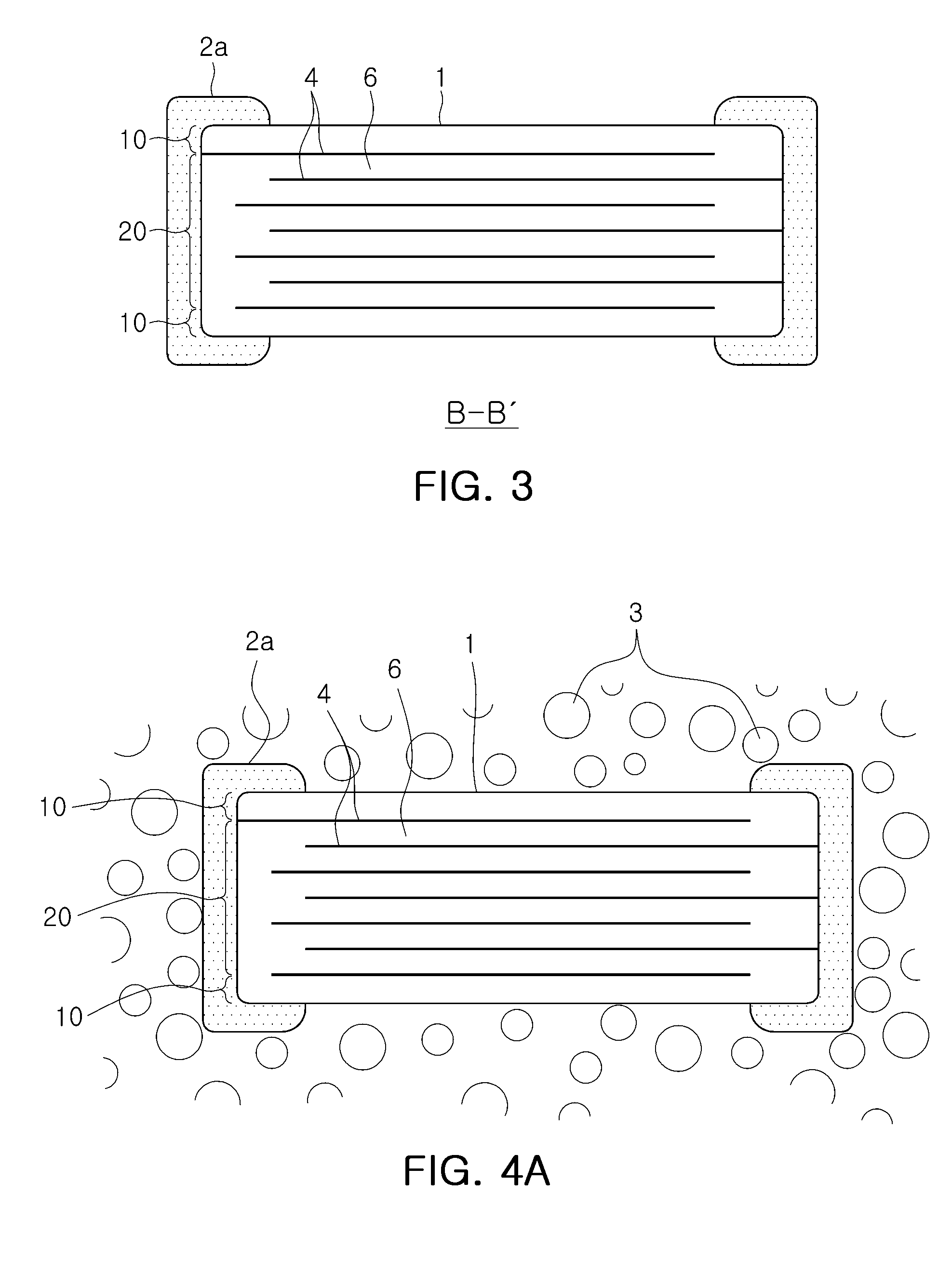
[0057]As shown in FIG. 4A, dielectric layers 6 of a capacitor body 1 were formed to include a binder, a plasticizer, and a residual dielectric material. The dielectric layers 6 were obtained by molding slurry including the constituent materials. Conductive internal electrodes 4 including nickel were printed on the dielectric layers 6, respectively. Then, the printed dielectric layers 6 were used to manufacture a lamination body having a predetermined thickness.

[0058]Next, the external electrode material layers 2a including copper were formed on the capacitor body 1. Then, the capacitor body 1 was dry polished by using zirconia ceramic balls 3. As a result, the surfaces of the external electrode material layers 2a became smooth and compact. Herein, the ceramic balls may be made of at least one selected from zirconia, alumina, and silicon carbide, but a material for forming the ceramic balls 3 is not limited thereto.

example 2

[0059]As in the example 1, a capacitor body 1, of which the surface was dry polished by using zirconia balls 3, was manufactured. Then, as shown in FIG. 4B, external electrodes 2 were completed by respectively forming plating layers 2b made of copper on the surfaces of external electrode material layers 2a which had been dry polished by zirconial balls 3 to be smooth and compact. Herein, the plating layers 2b made of copper were formed to have a thickness of 10 μm. The plating layers 2b were made of copper (Cu).

example 3

[0060]As in the example 2, external electrodes 2 werecompleted by respectively forming plating layers 2b made of copper on the surfaces of external electrode material layers 2a of a capacitor body 1, of which the surface was dry polished. Then, the plating layers 2b were plated with nickel (Ni) and tin (Sn) in order to more precisely observe the smoothness thereof.


PUM

PropertyMeasurementUnit
thicknessaaaaaaaaaa
thicknessaaaaaaaaaa
thicknessaaaaaaaaaa

Abstract

There are provided a multilayer ceramic capacitor, a printed circuit board including the same, a method of manufacturing the multilayer ceramic capacitor, and a method of manufacturing the printed circuit board. The method of manufacturing a multilayer ceramic capacitor includes: preparing a capacitor body on which external electrode material layers are formed, dry polishing the capacitor body such that surfaces of the external electrode material layers are smooth and compact, and forming plating layers on the surfaces of the external electrode material layers in order to form external electrodes. Therefore, the surface smoothness, compactness, and uniformity of an external electrode plating layer can be improved.

Description

CROSS-REFERENCE TO RELATED APPLICATIONS[0001]This application claims the priority of Korean Patent Application No. 10-2010-0041566 filed on May 3, 2010, in the Korean Intellectual Property Office, the disclosure of which is incorporated herein by reference.BACKGROUND OF THE INVENTION[0002]1. Field of the Invention[0003]The present invention relates to a multilayer ceramic capacitor, a printed circuit board including the same, and methods of manufacturing thereof, and more particularly, to a multilayer ceramic capacitor having improved surface smoothness, compactness, and uniformity of an external electrode plating layer, a printed circuit board including the same, a method of manufacturing the multilayer ceramic capacitor, and a method of manufacturing the printed circuit board.[0004]2. Description of the Related Art[0005]Compactness, thinness and high capacity have increasingly been required in a chip device, such as a multilayer ceramic capacitor (MLCC), a chip resistor, and a chi...

Claims


Application Information

Patent Timeline
Patent Type & Authority Applications(United States)
IPC IPC(8): H05K1/18H05K3/30H01G4/228H01G2/06H01G4/12H01G4/232H01G4/30
CPCH01G4/005H01G4/232H01G4/30H01G13/006H05K1/183Y10T29/4913H05K2201/09827H05K2201/10015H05K2203/1469Y10T29/43H05K1/185
Inventor KIM, GO EUNLIM, DONG CHUNSEO, YONG WON
Owner SAMSUNG ELECTRO MECHANICS CO LTD
Why Eureka
Try Eureka