Large capacity solid-state storage devices and methods therefor

Active Publication Date: 2011-11-17
KIOXIA CORP
View PDF8 Cites 23 Cited by
  • Summary
  • Abstract
  • Description
  • Claims
  • Application Information

AI Technical Summary

Benefits of technology

[0011]According to a second aspect of the invention, a method is provided for increasing addressable memory space of a non-volatile storage device that comprises a circuit board and control logic and non-volatile solid-state memory devices on the circuit board. The method includes providing multiple channels of the memory devices that are functionally arranged to define at least two banks of the memory devices per channel on the circuit board, providing the control logic to comprise system interface logic, a memory controller and channel control units integrated in a single integrated circuit package, providing bank switching circuitry associated with each channel and integrated on the single integrated circuit package, and operating the bank switching circuitry to multiply memory space within the memory devices that is addressable by each channel by the number of the at least two banks.
[0014]Each of the capabilities described above is achieved using the bank switching circuitry to duplicate control, address and data lines and act as an intermediate buffer for memory addresses before propagating them to multiple banks of memory devices using dedicated address and data lines on a per bank basis. Moreover, the bank switching circuitry can contain data buffers to buffer reads and writes from and to the memory banks and transfer them to the controller at n times the data rate between the bank switching circuitry and the memory device wherein n equals the number of banks enabled by the switching circuitry. As a result, the invention enables at least doubling of the capacity of a solid state drive without the need of an extra controller in an internal redundant array of independent drives (RAID) Level 0 configuration and further at least doubles the overall data transfer rate between the controller and the memory devices on each channel.

Problems solved by technology

Current solid state drives are limited in their capacity by the density of the NAND chips in conjunction with the limitations of the control logic, that is, the memory controller.
Even if the memory management unit is aware of a large memory space through, for example, a 48-bit large block addressing scheme, the actual controller will typically have limitations in the number of address lines or chip-enable lines, which then limits the overall capacity of the device to a much smaller size.
In the past, the cost of NAND flash memory was prohibitive for even considering ultra-high capacity solid state drives, but with production ramping up and NAND cost decreasing on average by 50% per year, solid state drives have not only gained acceptance in the market but are also constantly increasing in capacity.
Functionally, the RAID 0, as the most commonly used, will not be able to play out the combined transfer rates of two drives because the system interface (connector 14) is usually a single SATA link, which limits the host transfer rate and can cause some problems if the combined internal media transfer rate at the back-end of the solid state drive 10 is greater than the host transfer rate.
NAND flash is inherently slow because of its architecture and design limitations whereas flash controllers can be scaled up to outpace the performance of the memory components by multiples.

Method used


Image

  • Large capacity solid-state storage devices and methods therefor
  • Large capacity solid-state storage devices and methods therefor
  • Large capacity solid-state storage devices and methods therefor

Examples


Embodiment Construction

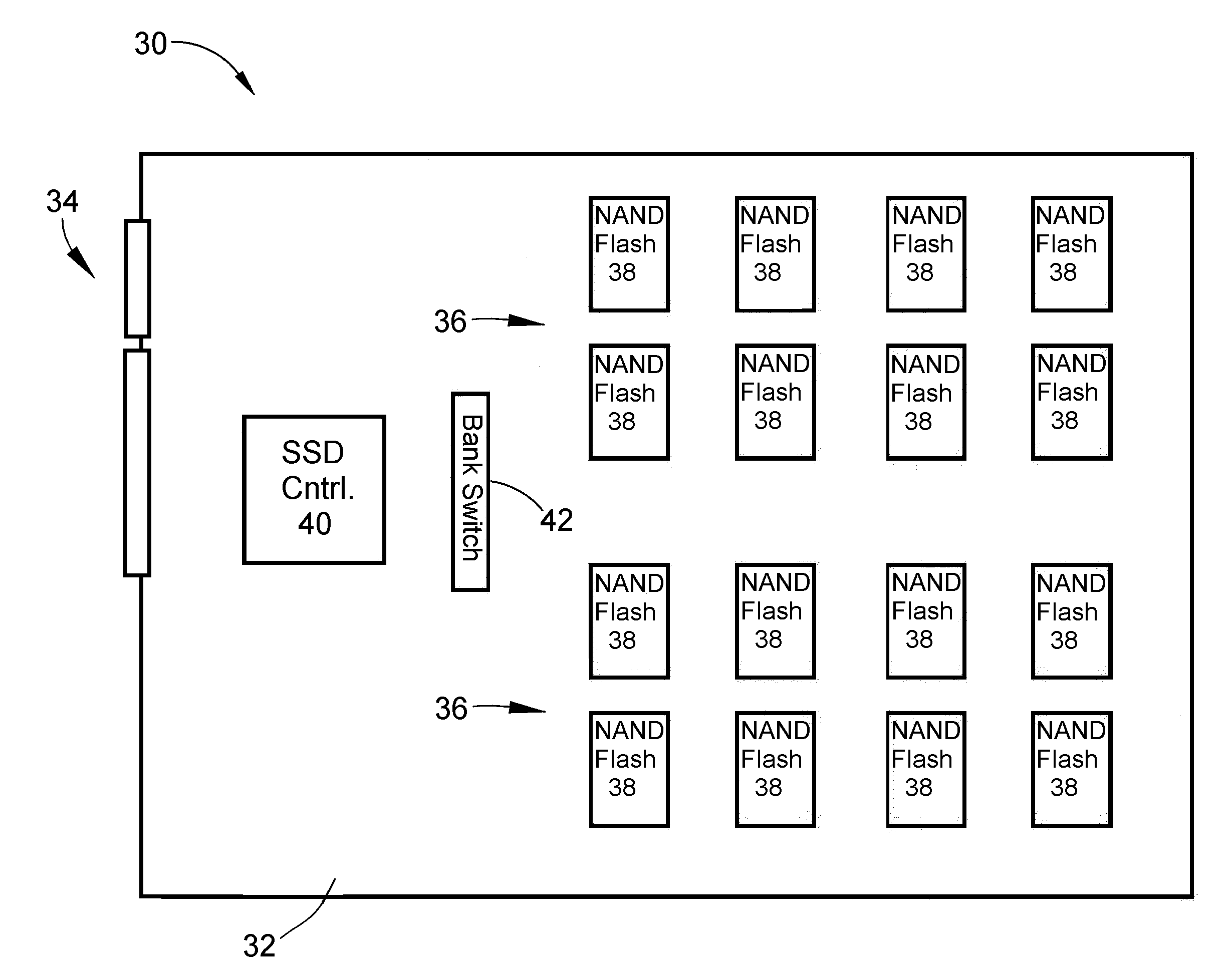
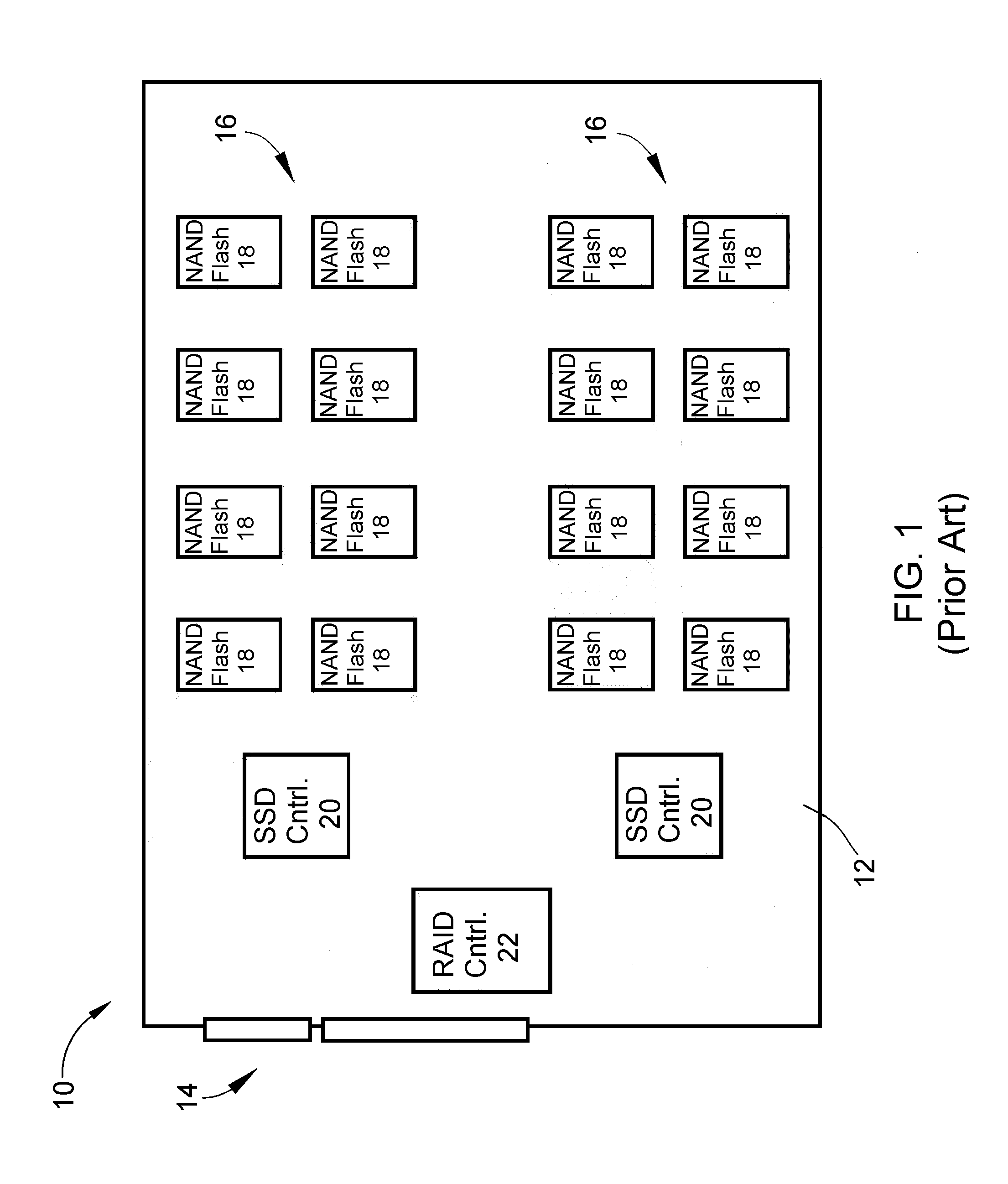
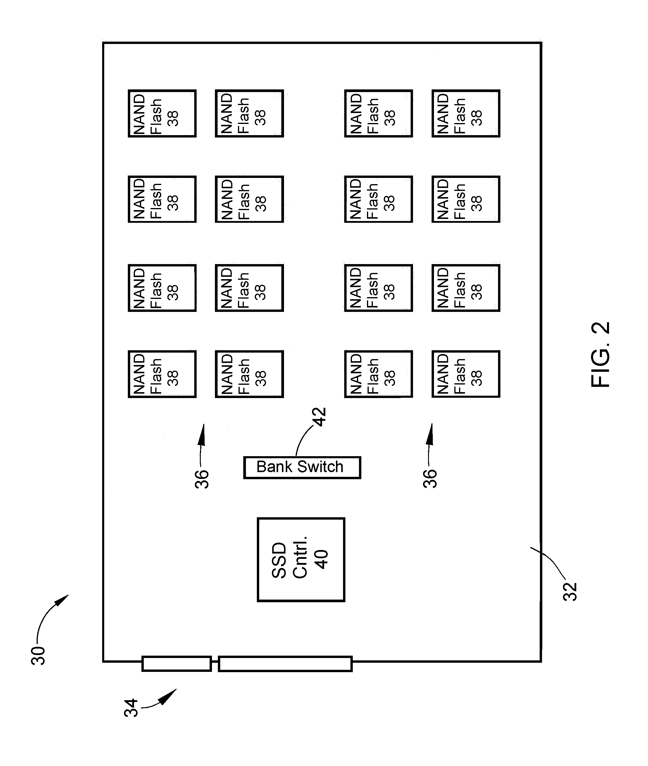
[0021]The present invention is generally applicable to computers and other processing apparatuses, and particularly to personal computers, workstations and other apparatuses that utilize nonvolatile (permanent) memory-based mass storage devices, a notable example of which are solid-state drives (SSDs) that make use of NAND flash memory devices. FIGS. 2, 3, and 4 schematically represent solid state drives configured as internal mass storage devices for a computer or other host system (not shown) equipped with a data and control bus for interfacing with the solid state drives. The bus may operate with any suitable protocol in the art, a preferred example being the serial advanced technology attachment (SATA) bus, though other protocols are also possible.

[0022]Current flash controllers used in solid state drives have typically utilized a plurality of individual, parallel channels for individual addressing of each NAND flash memory device or a logical group of NAND flash memory devices....


PUM


Abstract

Non-volatile storage devices and methods capable of achieving large capacity solid state drives containing multiple banks of memory devices. The storage devices include a printed circuit board, at least two banks of non-volatile solid-state memory devices, bank switching circuitry, a connector, and a memory controller. The bank switching circuitry is integrated onto the memory controller and functionally interposed between the banks of memory devices and the front end of the memory controller. The bank switching circuitry operates to switch accesses by the memory controller among the at least two banks.

Description

CROSS REFERENCE TO RELATED APPLICATIONS[0001]This application is a continuation in part of U.S. patent application Ser. No. 12 / 876,937, which claims the benefit of U.S. Provisional Application No. 61 / 240,338, filed Sep. 8, 2009. The contents of these applications are incorporated herein by reference.BACKGROUND OF THE INVENTION[0002]The present invention generally relates to memory devices for use with computers and other processing apparatuses. More particularly, this invention relates to high capacity non-volatile or permanent memory-based mass storage devices of the type known as solid state drives (SSD).[0003]Mass storage devices such as advanced technology (ATA) or small computer system interface (SCSI) drives are rapidly adopting non-volatile memory technology such as flash memory or other emerging solid state memory technology, including phase change memory (PCM), resistive random access memory (RRAM), magnetoresistive random access memory (MRAM), ferromagnetic random access m...

Claims


Application Information

Patent Timeline
IPC IPC(8): G06F12/06G06F12/02
CPCG06F3/0626G06F3/0658G06F2212/7208G06F12/0246G06F3/0679
Inventor SCHUETTE, FRANZ MICHAEL
Owner KIOXIA CORP
Why Eureka
Try Eureka