Quantum dot light emitting element and method for manufacturing the same

a light emitting element and quantum dot technology, applied in the field of method for manufacturing the same, can solve the problems of increasing the disadvantageous manufacture cost of the the limitation of the organic light emitting diode of presenting a variety of colors magnificently, and the complex structure of the conventional quantum dot light emitting element, etc., to achieve the effect of reducing the manufacture cost of the quantum light emitting device, improving yield and simple structure of the quantum do

Active Publication Date: 2011-11-24
LG DISPLAY CO LTD +1
View PDF7 Cites 54 Cited by
  • Summary
  • Abstract
  • Description
  • Claims
  • Application Information

AI Technical Summary

Benefits of technology

[0013]An object of the present invention is to provide a quantum dot light emitting element which forms a quantum light emitting layer and a charge transporting layer in a solution process which disperses charge transporting particles and quantum dots in a solvent to simplify a structure thereof and to reduce manufacture cost thereof, and a method for manufacturing the same.
[0032]Therefore, the quantum dot light emitting element according to the present invention has following effects.
[0033]First, the quantum light emitting layer is formed of mixture having the charge transporting particles and the quantum dots dispersed in a solvent. The structure of the quantum dot light emitting element is simple, with three layers or less. As a result, a yield may be improved.
[0034]Second, the quantum light emitting layer and the charge transporting layer are formed in the solution process. As a result, manufacture cost of the quantum light emitting device may be reduced. Especially, a process line used to manufacture a liquid crystal display device and other flat display devices may be applied to manufacture the quantum dot light emitting element according to the present invention.

Problems solved by technology

The organic light emitting diode has limitation of presenting a variety of colors magnificently.
However, such the conventional quantum dot light emitting element is configured of four or more layers except an electrode and the structure of the conventional quantum dot light emitting element is complex.
As a result, manufacture cost of the quantum dot light emitting element might be increased disadvantageously and process time might be increased.

Method used


Image

  • Quantum dot light emitting element and method for manufacturing the same
  • Quantum dot light emitting element and method for manufacturing the same
  • Quantum dot light emitting element and method for manufacturing the same

Examples


first embodiment

[0049]FIG. 2 is a sectional view of a quantum dot light emitting element according to a first embodiment of the present invention.

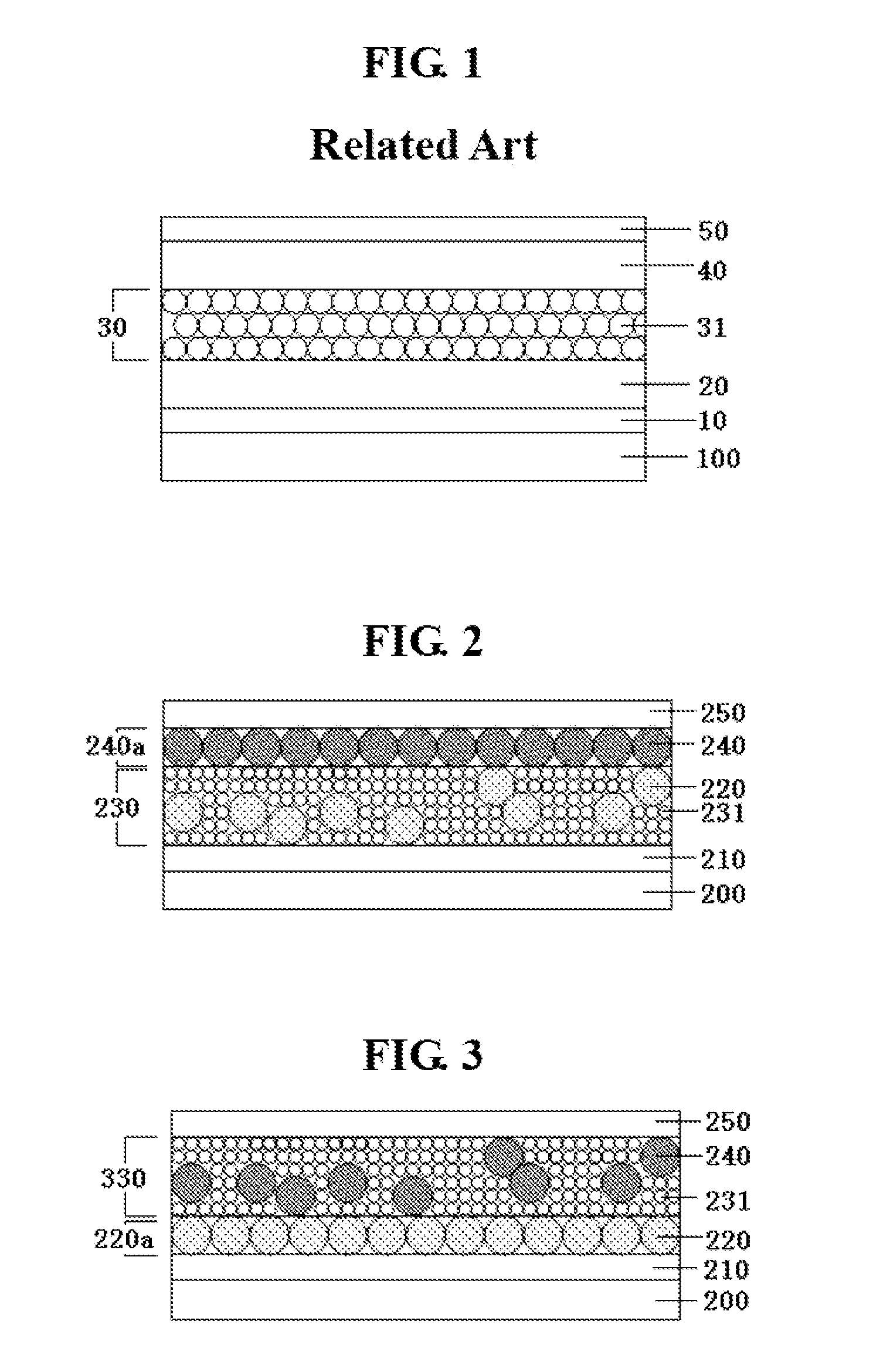
[0050]In reference to FIG. 2, the quantum dot light emitting element according to the first embodiment of the present invention includes a substrate 200, an anode 210 formed on the substrate 200, a quantum light emitting layer 230 formed on the anode 210, having p-type semiconductor nanoparticles 220 and quantum dots 231 mixed therein, and a cathode 250 formed on the quantum light emitting layer 230.

[0051]An electron transporting layer 240a may be further formed between the quantum light emitting layer 230 and the cathode 250.

[0052]The substrate 200 may be various types of substrates, not limited specifically, for example, a glass substrate, a plastic substrate and a silicon substrate. The anode 210 is configured of a transparent electrode selected from indium tin oxide, zinc oxide, indium oxide, tin oxide, indium zinc oxide. The cathode 250 is configured...

second embodiment

[0059]FIG. 3 is a sectional view of a quantum dot light emitting element according to a second embodiment of the present invention.

[0060]At this time, the same numeral references are given to the same components as those of the above embodiment described in reference to FIG. 2 and only different characteristic configuration will be described as follows to avoid repeated description.

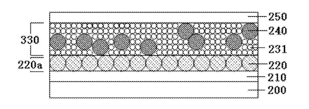
[0061]In reference to FIG. 3, the quantum dot light emitting element according to the second embodiment of the present invention includes a substrate 200, an anode 210 formed on the substrate 200, a quantum light emitting layer 330 formed on the anode 210, having n-type semiconductor nanoparticles 220 and quantum dots 231 mixed therein, and a cathode 250 formed on the quantum light emitting layer 330.

[0062]A hole transporting layer 220a may be further formed between the quantum light emitting layer 330 and the anode 210.

third embodiment

[0063]FIG. 4 is a sectional view of a quantum dot light emitting element according to a third embodiment of the present invention.

[0064]At this time, the same numeral references are given to the same components as those of the above embodiment described in reference to FIG. 2 and only different characteristic configuration will be described as follows to avoid repeated description.

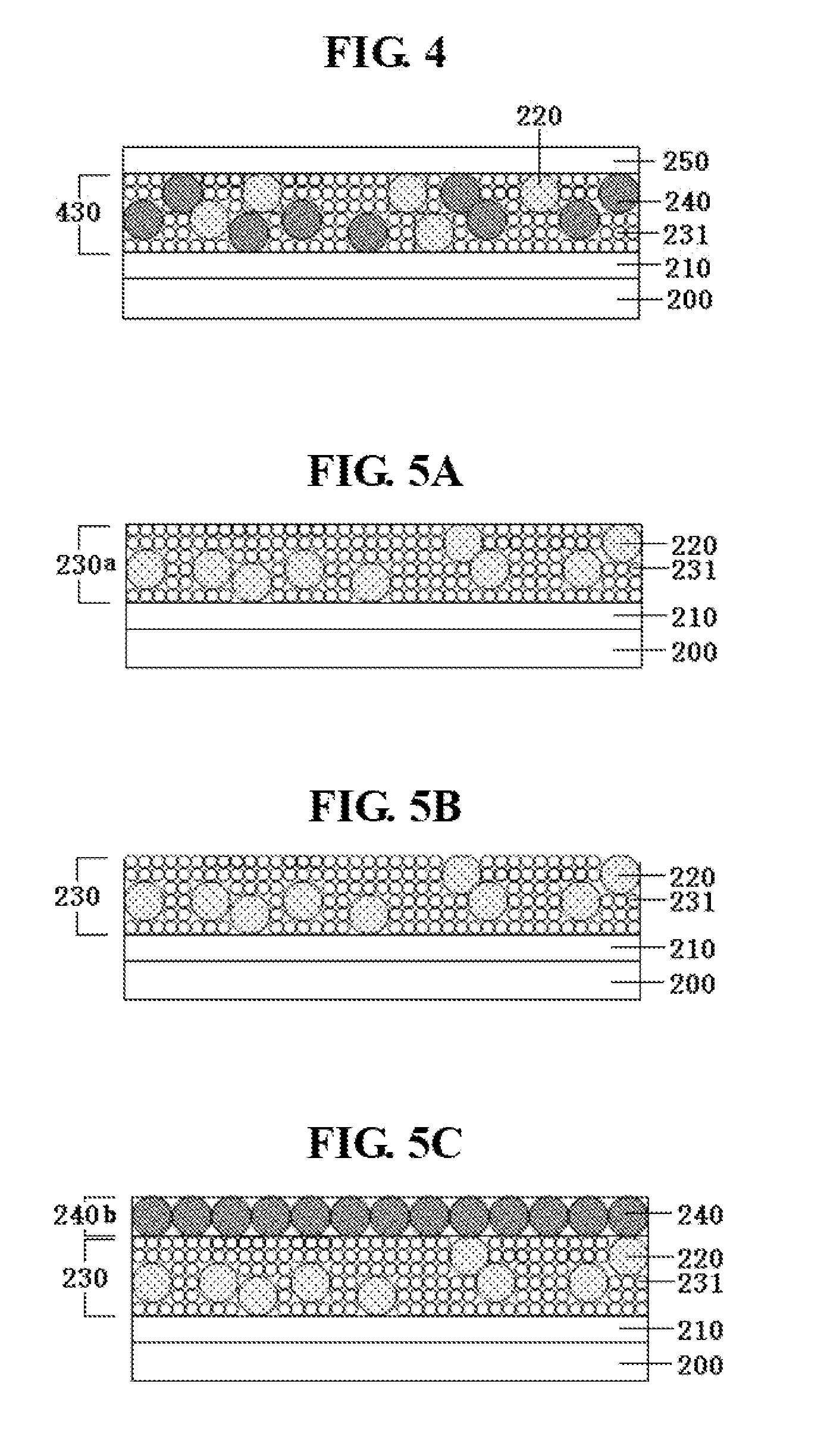
[0065]In reference to FIG. 4, the quantum dot light emitting element according to the third embodiment of the present invention includes a substrate 200, an anode 210 formed on the substrate 200, a quantum light emitting layer 430 formed on the anode 210, having n-type semiconductor nanoparticles 240, p-type semiconductor nanoparticles 220 and quantum dots 231 mixed therein, and a cathode 250 formed on the quantum light emitting layer 430.

[0066]As follows, a method for manufacturing the quantum dot light emitting element according to the embodiments of the present invention will be described.

[0067]FIGS. 5a...


PUM


Abstract

The present invention relates to a quantum dot light emitting element which can form a quantum light emitting layer configured of charge transporting particles and quantum dots and a charge transporting layer in a solution process, to reduce process expense, and a method for manufacturing the same. The quantum dot light emitting element includes a substrate, an anode formed on the substrate, a quantum light emitting layer formed on the anode, the quantum light emitting layer having charge transporting particles and quantum dots mixed therein, and a cathode formed on the quantum light emitting layer.

Description

CROSS REFERENCE TO RELATED APPLICATION[0001]This application claims the benefit of the Patent Korean Application No. 10-2010-0047397, filed on May 20, 2010, which is hereby incorporated by reference as if fully set forth herein.BACKGROUND OF THE DISCLOSURE[0002]1. Field of the Disclosure[0003]The present invention relates to a quantum dot light emitting element which can form a quantum light emitting layer configured of charge transporting particles and quantum dots and a charge transporting layer in a solution process, to reduce process expense, and a method for manufacturing the same.[0004]2. Discussion of the Related Art[0005]Quantum dot (QD) is a semiconductor nanoparticle, with the quantum dot of a nanometer size emits a light when an electron of an unstable state is moving downward to a valence band from a conduction band. As a particle of the quantum dot is smaller, a light having a shorter wavelength is generated. As the particle of the quantum is larger, a light having a lo...

Claims


Application Information

Patent Timeline
Patent Type & Authority Applications(United States)
IPC IPC(8): H01L33/04B82Y40/00B82Y99/00
CPCB82Y20/00H01L21/02601H01L51/502H05B33/10H10K50/115H10K71/12
Inventor KANG, HO-CHEOLNOH, YOUNG-HOONLEE, CHANG-HEECHAR, KOOK HEONLEE, SEONG-HOONKWAK, JEONG HUNBAE, WAN KILIM, JAE HOONLEE, DONG GU
Owner LG DISPLAY CO LTD
Why Eureka
Try Eureka