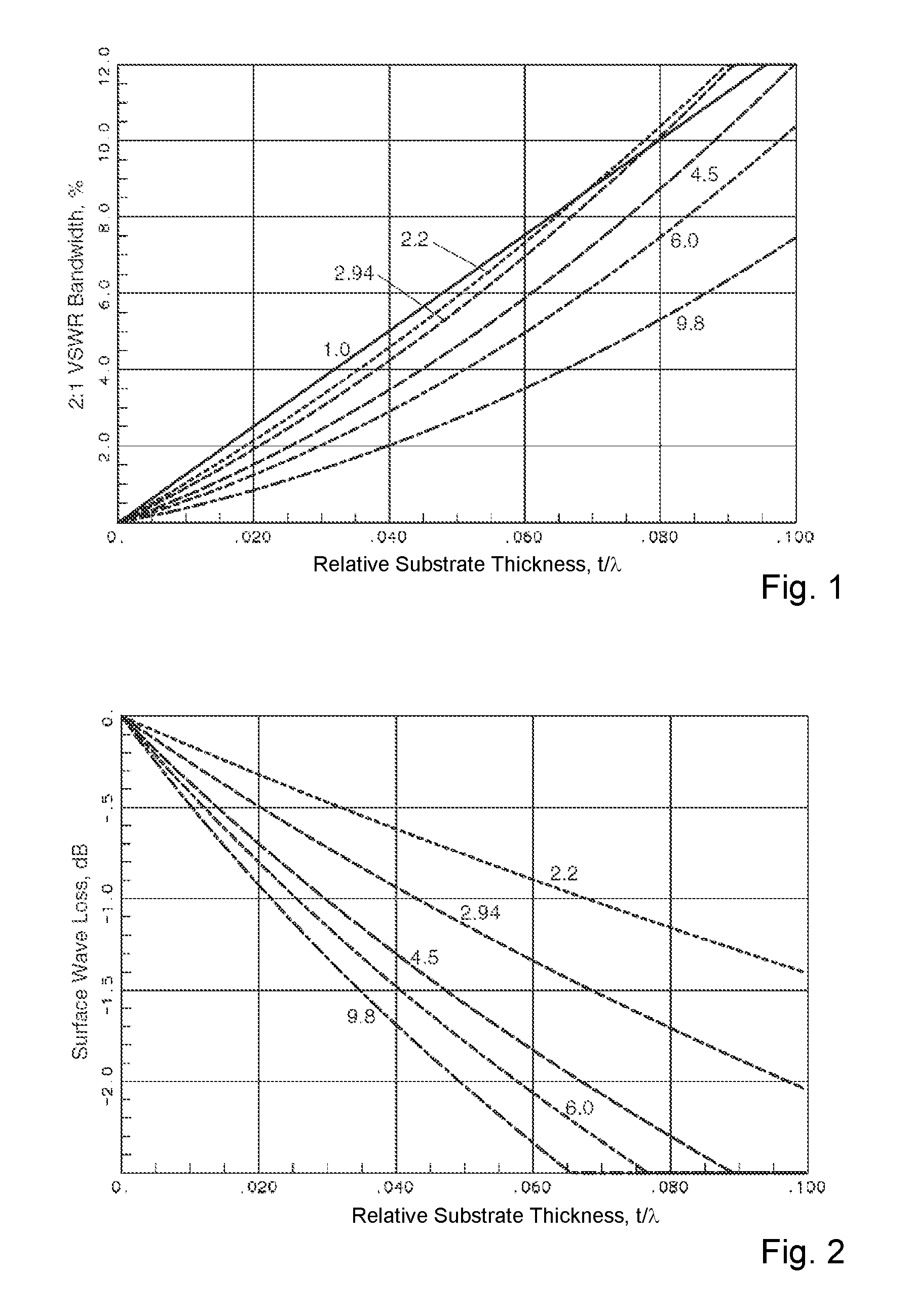
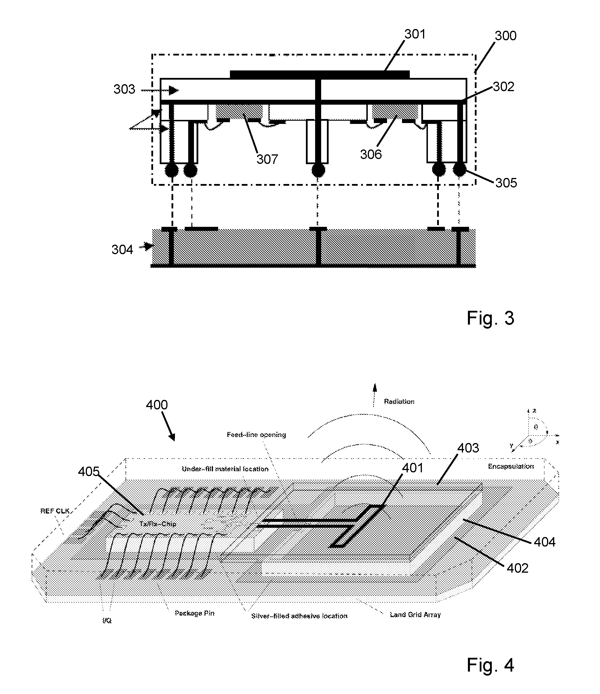
[0053]FIGS. 1 to 5 have already been discussed above in relation to the background to the invention.
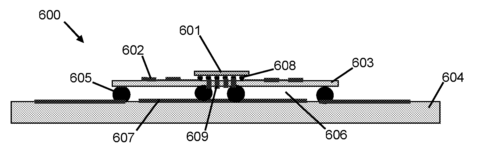
[0054]An embodiment of an antenna module package 600 according to the invention is illustrated in a schematic cross-section shown in FIG. 6. The package 600 comprises an active semiconductor die 601 and a micro-strip antenna 602 formed on a standard BT (Bismaleimide Triazine) epoxy laminate substrate 603. The die 601 is mounted on the same substrate 603 as the antenna 602, and the antenna substrate 603 is mounted on an underlying substrate or motherboard 604 by means of a ball grid array comprising an array of conductive balls 605.
[0055]An important feature of the antenna module construction shown in FIG. 1 is the use of the air dielectric gap 606 between the antenna substrate 603 and a ground plane 607 on the motherboard 604. The air gap 606 acts as a high quality dielectric medium for the micro-strip antenna 602. This method of construction results in various advantages, detailed as follows.
[0056]The low dielectric constant and low loss of the air gap 606 (∈r=1, tan δ=0) is ideal for micro-strip antennas due to the improvements in impedance bandwidth and surface wave efficiency, as demonstrated in FIGS. 1 and 2.
[0057]The additional effective antenna volume created by the use of the, otherwise wasted, volume of the gap between the package and the board offers increased bandwidth performance without an increase in package area or height.
[0058]The extra effective antenna volume is created without increasing the surface area (or aperture) of the antenna 602, which would increase the directivity of the elements and in this way limit the range of angles over which the array can be scanned. The large scanning range possible using an antenna module according to an embodiment of the invention is shown in FIGS. 10a-c.
[0059]The antenna module 600 is suitable for use with standard laminate materials as the antenna substrate. The dielectric properties of the combination of a thin dielectric layer with a thick air gap tend to be dominated by the properties of the air layer. This significantly relaxes the requirements on the dielectric constant and dielectric loss of the antenna substrate 603.
[0060]The antenna module is also suitable for use in a standard BGA assembly process. The thickness of the air dielectric 606 is determined by the stand-off height of the package, which is a well-controlled parameter in high volume assembly processes.
[0061]A second important feature of the antenna module 600 is that connections between the transceiver module 601 and antenna 602 can be simplified. Metal traces provided on the surface of the antenna substrate 603 can connect directly to a smaller ball grid array connecting the transceiver die 601 to the antenna substrate 603 via solder balls 608. The antenna 602 is therefore preferably provided on the same face of the substrate 603 to which the transceiver module 601 is mounted. These features offer further advantages compared to more complex interconnect structures, including: i) a larger frequency bandwidth and lower signal loss due to reduced parasitic effects; ii) reduced coupling between the elements of a phased array antenna structure, which improves gain in the desired direction and suppress gain in the direction of interference; and iii) the construction is simpler to model, thus reduces design time.
[0062]A further feature of the antenna module embodiment illustrated in FIG. 6 is that of embedding a low thermal resistance path between the active die 601 and the ground plane 607 of a circuit board forming an underlying substrate or motherboard 604. This can be achieved through combining the smaller ball grid array mounting the die 601 to the antenna substrate with an array of thermal vias 609 passing through the antenna substrate 603 and in thermal communication with an inner portion of the larger ball grid array connecting the antenna substrate 603 with the motherboard 604. This combination of features functions as a heat sink, thereby limiting the maximum device temperature of the die 601, which is particularly important when applied to power intensive circuits such as power amplifiers and high speed digital circuits. The maximum operating temperature can be directly related to the lifetime of these circuits, so any step to reduce this can prolong the life of the module 600.
[0063]A particular application of the antenna module is in the integration of a transceiver chip with a phased array antenna for mm-wave communication, radar or imaging applications. FIG. 7 (not to scale) illustrates an example of such an application, in the form of a cross-sectional view (FIG. 7a) and a plan view (FIG. 7b) of a module comprising a 60 GHz wireless HDMI transceiver die together with a four element linear phased array antenna with half wavelength (λ/2) element spacing. The cross-sectional view in FIG. 7a is similar to the antenna module 600 shown in FIG. 6, and corresponding reference signs apply.
[0064]The antenna array 602 is formed on a standard BT laminate substrate 603, with ∈r=3.8 and tan δ=0.01. A mm-wave interconnect to the transceiver IC 601 is realised with a grid of 100 μm diameter solder balls 608. A grid of 500 μm diameter solder balls 605 is used to define the air dielectric gap between the antenna 602 and the ground plane 607, and also for a low frequency interconnect between the transceiver IC and the motherboard 604.
[0065]As shown in FIG. 7a, the thickness 710 of the air dielectric gap is greater than the thickness 720 of the antenna substrate, thereby allowing the dielectric properties of the air gap 606 to dominate. The air gap thickness 710 is preferably at least twice the thickness 720 of the antenna substrate. A typical thickness of the antenna substrate is around 200 μm, while the air gap thickness may be around 500 μm, for example between 400 and 600 μm for operation at 60 GHz, corresponding to a free space wavelength of 5 mm.
[0066]The antenna array 602 comprises four antenna elements 602a-d, the elements being spaced from each other by a half wavelength, in this case by 2.5 mm (λ=5 mm, f=60 GHz). Each of the antenna elements is in the form of a folded dipole, and has a span 701 of 1.5 mm.
[0067]The larger BGA comprises an outer ring 702 of balls surrounding the antenna array 602, and an inner grid 703 of balls connecting the transceiver IC 601, both electrically and thermally, to the motherboard 604. The smaller BGA 704 shown in FIG. 7b connects the transceiver IC 601 (not shown in FIG. 7b) to the antenna substrate 603.
[0068]The performance of the antenna array 602 has been analysed by performing a number of electro-magnetic simulations. FIGS. 8a and 8b show the impedance bandwidth of a single folded dipole element for a nominal air dielectric gap thickness of 400 μm, 500 μm and 600 μm to investigate the effect of process spread. Points m1 and m2 on FIG. 8b indicate where the measured VSWR=2 for a 500 μm air gap, point m1 being at 54.5 GHz, point m2 being at 67.9 GHz. The nominal 2:1 VSWR impedance bandwidth is over 15% for each of the thicknesses of air gaps shown, thereby demonstrating the wide bandwidth capability of the antenna module.
[0069]FIGS. 9a and 9b show results from a simulation of radiation efficiency (FIG. 9a) and directivity (FIG. 9b) of a single folded dipole element of the antenna module. These results indicate that less that 20% of the power is lost in surface waves and dissipation in the dielectric and conductors, and demonstrate that air acts as an efficient antenna dielectric. The directivity of the antenna is mainly created by the ground-plane beneath the antenna, which acts as a reflector to concentrate the transmitted radio energy in a direction orthogonal to the ground plane and antenna substrate.
[0070]FIGS. 10a to 10c show results of the directivity of the antenna module of FIG. 7, as a function of scan angle θ, in the cases where the phase of the input signals are selected for maximum radiation in the directions θ=0° (FIG. 10a), θ=30° (FIGS. 10b) and θ=60° (FIG. 10c), the value for θ indicating the angle with respect to the normal to the plane of the antenna substrate. The possibility of scanning over such a large range is related to the relatively large distance between the antenna and the ground plane in the antenna module.
[0071]FIG. 11 illustrates an alternative embodiment of an antenna module 1100, in which the antenna array 602 is provided on a face of the antenna substrate opposing the face on which the semiconductor die 601 is mounted. Interconnections between the die 601 and the antenna array 602 are achieved by means of via connections 1110. The remaining features of the module 1100 are otherwise similar to those of the embodiment in FIG. 6 described above. Having the antenna array 602 on the underside of the antenna substrate 603, i.e. using the antenna substrate 603 as a superstrate for the antenna 602, offers the possibility of increasing the gain per element of the array, at the cost of a reduction in angular coverage. This particular embodiment would therefore be more suitable for fixed beam applications.
[0072]FIG. 12a shows a further alternative embodiment of an antenna module 1200, in which the semiconductor die 601 is mounted on the same face as the antenna array 602, but with both mounted on the underside of the antenna substrate and on the same face as the ball grid array 605. As compared with the embodiment of FIG. 11, interconnections between the die 601 and antenna array 602, as well as between the die and the underlying circuit board 604, are simplified, requiring no via connections through the antenna substrate 603. As with the embodiment of FIG. 11, using the antenna substrate 603 as a superstrate for the antenna 602 offers the possibility of increasing the gain per element of the array, at the cost of a reduction in angular coverage. The overall module 1200 occupies even less space than the embodiments illustrated above. Because the die 601 is connected to the underside of the antenna substrate 603, thermal connections to the circuit board 604 are made via a heat pipe arrangement, illustrated in plan view in FIG. 12b. A thermally conductive heat pipe 1206 connected to an inner ball grid array 1205 conducts heat away from the die 601 into the circuit board 604. In this arrangement, the height of the semiconductor die 601 and smaller ball grid array 608 is restricted to the thickness provided by the larger ball grid array 605 connecting the antenna substrate 603 to the circuit board 604 and defining the air dielectric gap 606 between the antenna 602 and the ground plane 607 on the circuit board 604.
[0073]Other potential applications of the proposed antenna module include integration of other types of micro-strip- or slot-radiators (e.g. open dipole, patches, cavity backed slots etc.), and integration of other array configurations (e.g. rectangular arrays, circular arrays etc.).
[0074]Antenna modules of the type described herein can be used for low cost packaging of integrated circuits and antennae (or antenna arrays) for mm-wave communication, radar and imaging systems. A first example is the use in 60 GHz wireless systems for distribution of high quality streaming video signals, or for the transfer of ultra high bit-rate data streams. A second example is the use in 77 GHz car radar systems for adaptive cruise control. A third example is the use of this concept above 100 GHz for imaging based security systems.
[0075]Other embodiments are intentionally within the scope of the invention as defined by the appended claims.
REFERENCES
[0076] [1] Constantine A. Balanis, “Antenna Theory 3rd ed,”, ISBN-0-471-66782-X, pp. 811-812. [0077] [2] L. J. Chu, “Physical limitations of omni-directional antennas”, J. Applied Physics, vol. 19, pp. 1163-1175, 1948. [0078] [3] D. R. Jackson and N. G. Alexopoulas, Simple approximate formulas for input resistance, bandwidth and efficiency of a resonant rectangular patch, IEEE Transactions on Antennas and Propagation, vol. 39, no. 3, March 1991, pp 407-410. [0079] [4] Khandelwal N. and Jackson R. W., “An X-band System-in-Package Active Antenna Module”, 0-7803-8846-1/05/$20.00(C) 2005 IEEE. [0080] [5] Pfeiffer U. R. et al, “A Chip-Scale Packaging Technology for 60 GHz Wireless Chipsets”, IEEE Transactions on Microwave Theory and Techniques, vol. 54, no. 8, August 2006, pp. 3387-3395. [0081] [6] Waterhouse R. B., “Microstrip Patch Antennas, A Designers Guide”, Kluwer Academic, Boston 2003. par. 3.6.