Solder bump formation on a circuit board using a transfer sheet

a transfer sheet and circuit board technology, applied in the field of forming solder bumps, can solve the problems of bridging between the electrodes, too much solder on the electrode portions, and excessive amount of solder, and achieve the effect of reducing the size of electronic equipmen

Active Publication Date: 2011-12-08
SENJU METAL IND CO LTD
View PDF7 Cites 20 Cited by
  • Summary
  • Abstract
  • Description
  • Claims
  • Application Information

AI Technical Summary

Benefits of technology

[0013]The present inventors confirmed that the transfer sheet described in Patent Document 2 can effectively form solder bumps with little variation on individual electrodes of a circuit board when using solder particles which have been classified to a particle diameter of 5-15 μm if the electrode pitch is 150 μm or larger. However, if the electrode pitch becomes smaller than this size, bridging develops between the electrodes. The cause of bridging is thought to be as follows. When solder particles are melted using a transfer sheet having solder particles adhered over its entire surface, the solder particles are melted not only in the portions which contact electrodes (electrode portions) but also in other portions (non-electrode portions). Therefore, when the electrodes are

Problems solved by technology

However, if the electrode pitch becomes smaller than this size, bridging develops between the electrodes.
Therefore, when the electrodes are wet by molten solder, molten solder on the n

Method used


Image

  • Solder bump formation on a circuit board using a transfer sheet
  • Solder bump formation on a circuit board using a transfer sheet
  • Solder bump formation on a circuit board using a transfer sheet

Examples


first embodiment

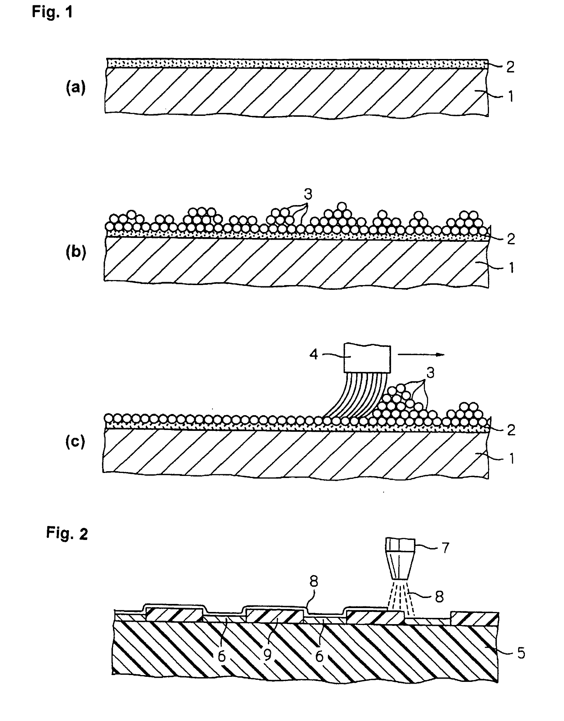
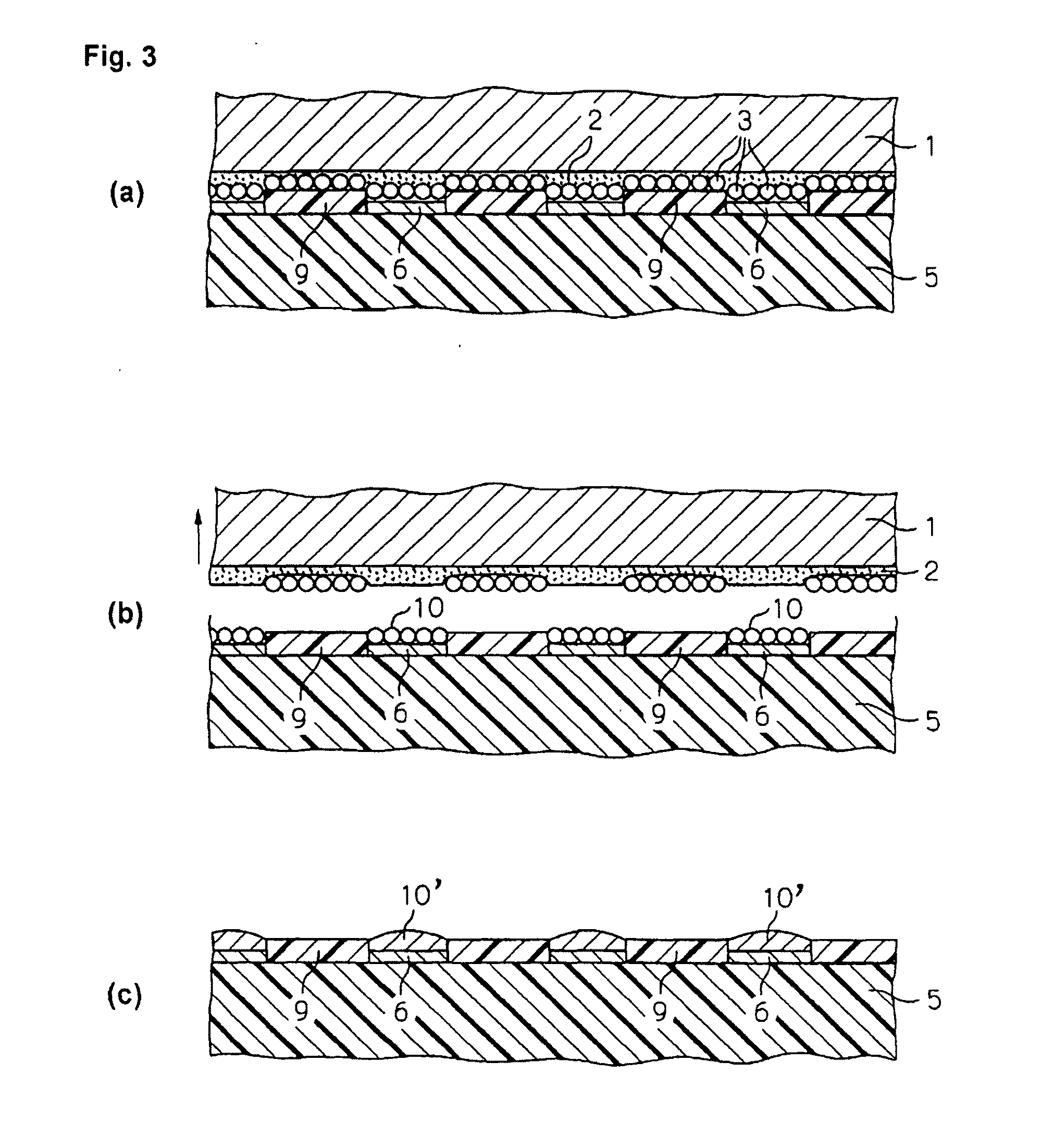
[0049]In a first embodiment of the present invention, a solder transfer sheet has a solder layer which is a solder particle layer formed from solder particles distributed in the form of a monoparticle layer. FIGS. 1(a)-1(c) are explanatory views showing a series of steps in a method of manufacturing a solder transfer sheet having a solder particle layer. A method of manufacturing this solder transfer sheet is the same as the method described in above-mentioned Patent Document 2, and it includes a step of forming an adhesive layer atop a supporting substrate (FIG. 1(a)), a step of dispersing solder particles atop the adhesive layer to adhere the solder particle layer to the adhesive layer (FIG. 1(b)), and a step of removing solder particles which are not adhered to the adhesive layer (FIG. 1(c)).

[0050]First, an adhesive layer 2 is formed atop a supporting substrate (FIG. 1(a)). The supporting substrate 1 is made from a material to which solder does not readily adhere and which has he...

second embodiment

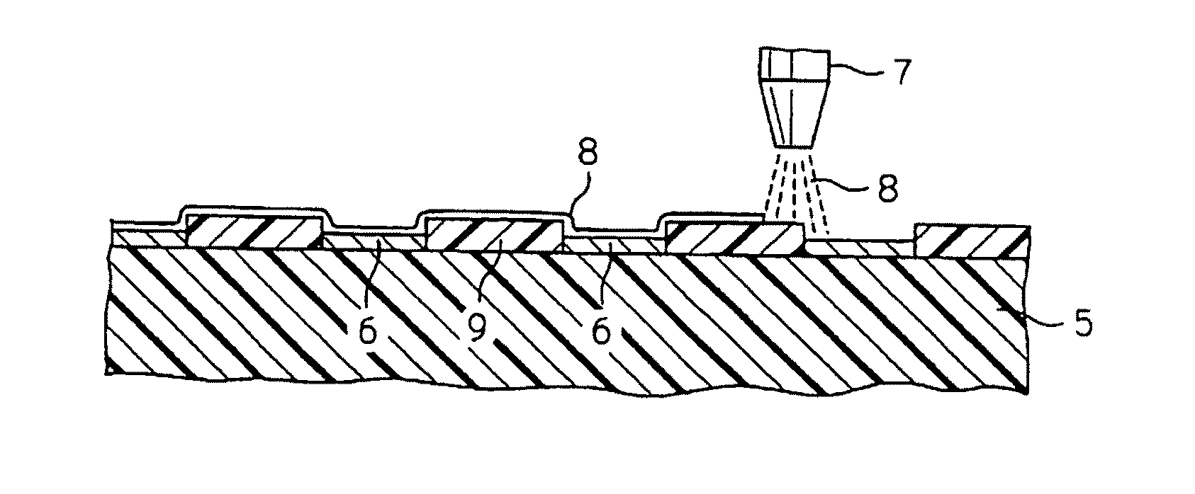
[0093]In a second embodiment of the present invention, a solder transfer sheet has a solder layer in the form of a continuous coating of a solder alloy. Below, the second embodiment of the present invention in which a solder layer is a continuous coating will be explained for the case in which the portions to be soldered of a circuit board have a surface made of Au. However, the portions to be soldered may have a surface of a metal or alloy other than Au such as Cu. In this case, an oxide film is present on the surface of the portions to be soldered, so the oxide film can be previously removed prior to bonding, or the above-described solid phase bonding flux can be provided at the bonding interface.

[0094]Electrodes of a circuit board which are soldered using a lead-free solder often have an Au plating layer provided atop an underlying Ni plating layer, so the surface of the electrodes is made of metallic Au. This type of electrode will be referred to below simply as an Au-plated ele...

example 1

[0131]This example illustrates the formation of solder bumps using a solder transfer sheet having a solder layer in the form of a monoparticle layer of solder particles.

[0132]A commercially available adhesive sheet (SBHF manufactured by Panac Industries, Inc.) having an adhesive layer with a thickness of 25 μm formed from an acrylic adhesive on one side of a polyester film (polyethylene terephthalate) with a thickness of 50 μm was cut to a size of 100×100 mm and used as a supporting substrate having an adhesive layer. The adhesive strength of the adhesive layer was measured by the 180° peeling adhesive strength measuring method prescribed by JIS Z 0237 and was found to be 7 N for a width of 25 mm.

[0133]As shown in FIGS. 1(b) and 1(c), solder particles obtained by classifying spherical powder of an Sn-3.5% Ag eutectic solder alloy (the solidus temperature and liquidus temperature were both 221° C.) to a particle diameter of from 5 μm to 10 μm were adhered to a thickness of one partic...


PUM

PropertyMeasurementUnit
Thicknessaaaaaaaaaa
Solidus temperatureaaaaaaaaaa
Temperatureaaaaaaaaaa

Abstract

A method of forming solder bumps on electrodes of a circuit board without producing bridging using a solder transfer sheet which does not require alignment includes superposing a circuit board and a solder transfer sheet having a solder layer adhered to at least one side of a supporting substrate, performing heating under pressure to a temperature lower than the solidus temperature of the solder to selectively perform solid phase diffusion bonding of the solder layer to electrodes, and peeling the transfer sheet from the circuit board. The solder layer is in the form of a continuous solder coating or in the form of a monoparticle layer of solder particles which are adhered to the supporting substrate by an adhesive layer.

Description

TECHNICAL FIELD[0001]This invention relates to a method of forming solder bumps by selective solid phase diffusion bonding to portions to be soldered of a circuit board using a transfer sheet and to a transfer sheet used in this method.[0002]The term “circuit board” used herein means a substrate on which electronic circuits are installed. It is exemplified by a printed circuit board, but it also encompasses the surface portions having electrodes of various electronic parts such as chip parts which are mounted on a printed circuit board. Electronic parts include active parts such as semiconductor elements, passive parts such as resistors and capacitors, and mechanical parts such as connectors.[0003]Examples of soldering of a circuit board are soldering of electronic parts to a printed circuit board and soldering of the electrodes of electronic parts to each other.[0004]A typical example of a portion to be soldered of a circuit board is an electrode on a circuit board. For example, po...

Claims


Application Information

Patent Timeline
IPC IPC(8): H05K1/11B32B5/00B32B15/04B23K1/20B23K35/24
CPCB23K1/0016Y10T428/265B23K35/262C22F1/00H01L21/4853H01L21/6835H01L2224/11003H01L2924/01002H01L2924/01013H01L2924/01027H01L2924/01029H01L2924/01033H01L2924/01047H01L2924/01078H01L2924/01079H01L2924/01082H01L2924/01322H01L2924/01327H01L2924/09701H01L2924/19041H05K3/3478H05K3/3484H05K2203/0338H05K2203/0405H05K2203/0425H01L2924/01005H01L2924/01006H01L2924/014H01L2924/00013B23K3/0638Y10T428/12736H05K2203/0415H05K2203/041H01L2224/131H01L2224/11332H01L2224/115H01L2224/29099Y10T428/31678H05K3/3485H05K3/34B23K1/20B23K3/06
Inventor KURAMOTO, TAKEOTSURUTA, KAICHISAITOU, TAKEO
Owner SENJU METAL IND CO LTD
Why Eureka
Try Eureka