Non-volatile memory and manufacturing method thereof

a manufacturing method and non-volatile memory technology, applied in the direction of basic electric elements, electrical apparatus, semiconductor devices, etc., can solve the problems of increasing process complexity, affecting the operation speed and charge storage capability of devices, etc., and achieves low operation voltage, no influence on device efficiency, and high efficiency of programming/erasing

Active Publication Date: 2012-01-26
UNITED MICROELECTRONICS CORP
View PDF3 Cites 17 Cited by
  • Summary
  • Abstract
  • Description
  • Claims
  • Application Information

AI Technical Summary

Benefits of technology

[0027]Owing to the present embodiments do not adopt the conventional solution of replacing the gate dielectric layer by the ONO structure, the present embodiments can be compatible with the current logic process and would not influence the efficiency of device. In addition, in the non-volatile memory of the present invention, a part of the nitride layer (charge trap layer) is formed between the gate conductive layer and the substrate, so that can avoid encountering the problem of electron drift and would not influence the operation speed and charge storage capability of device, and further can achieve relatively high efficiency of programming / erasing at low operation voltage. Moreover, the manufacturing method of the present invention would not increase the amount of photo mask and thus would not increase the process complexity.

Problems solved by technology

However, the planar type SONOS memory device uses the ONO structure to replace the gate oxide layer and thus is incompatible with the current logic process, and further would increase the process complexity so that the efficiency of device is influenced.
Therefore, during the sidewall type SONOS memory device is in operation, electrons are necessarily required to be injected into the silicon nitride charge trap layer, which would easily encounter the issue of electron drift and influence the operation speed and charge storage capability of device.
Owing to the present embodiments do not adopt the conventional solution of replacing the gate dielectric layer by the ONO structure, the present embodiments can be compatible with the current logic process and would not influence the efficiency of device.

Method used


Image

  • Non-volatile memory and manufacturing method thereof
  • Non-volatile memory and manufacturing method thereof
  • Non-volatile memory and manufacturing method thereof

Examples


Embodiment Construction

[0034]A better understanding of the above and many other features and advantages of the novel non-volatile memory and manufacturing method thereof of the present invention may be obtained from a consideration of the detailed description of some exemplary embodiments thereof below, particularly if such consideration is made in conjunction with the appended drawings, wherein like reference numerals are used to identify like elements illustrated in one or more of the figures thereof.

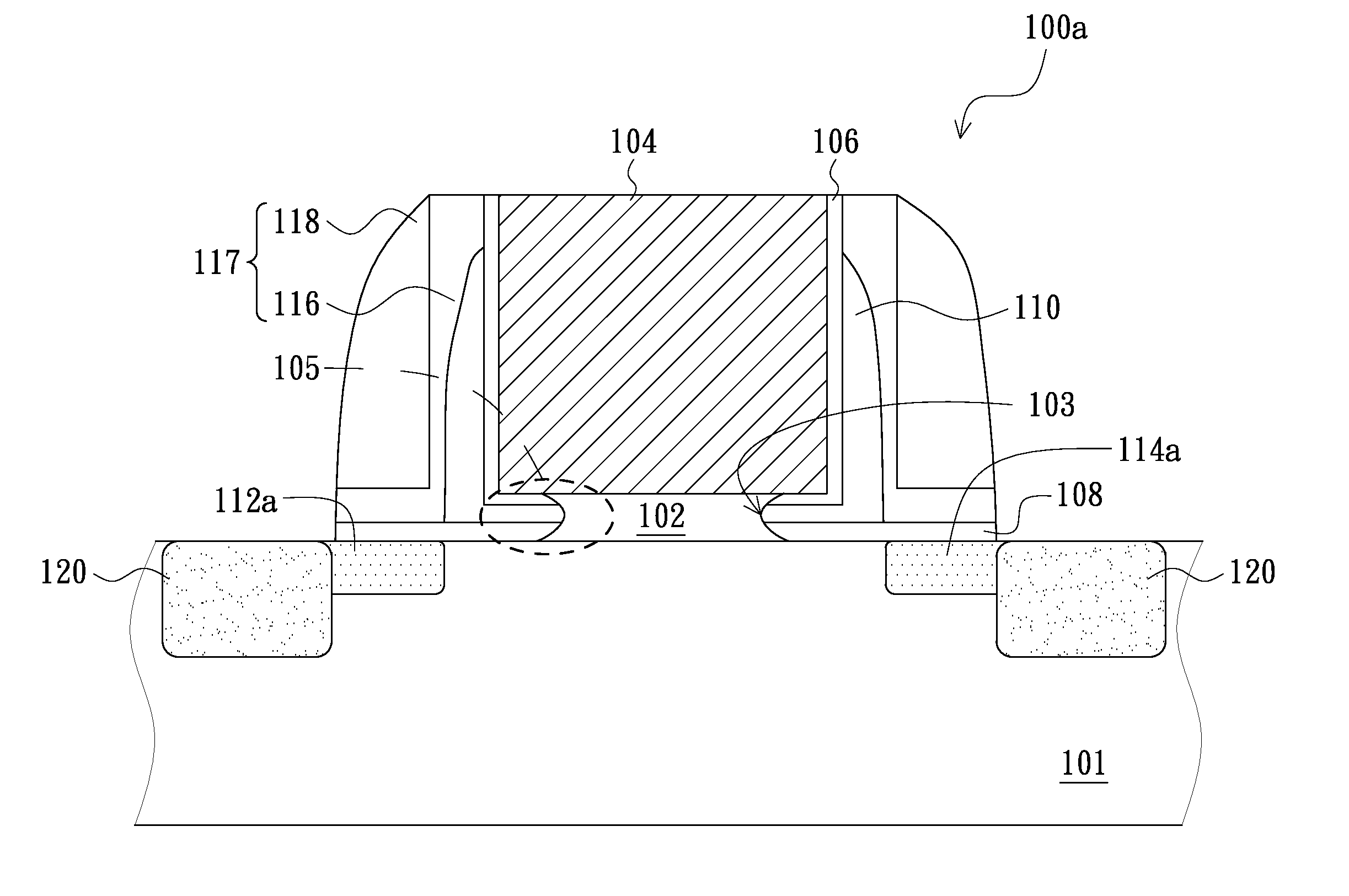
[0035]FIG. 1 illustrates a schematic cross-sectional view of a non-volatile memory in accordance with an embodiment of the present invention.

[0036]As illustrated in FIG. 1, the non-volatile memory 100 includes a substrate 101, a gate dielectric layer 102, a gate conductive layer 104, a first oxide layer 106, a nitride layer 110 and a second oxide layer 108. The substrate 101 is for example a silicon substrate. The gate dielectric layer 102 is disposed on the substrate 101. The gate dielectric layer 102 has ...


PUM


Abstract

A manufacturing method of a non-volatile memory is disclosed. A gate structure is formed on a substrate and includes a gate dielectric layer and a gate conductive layer. The gate dielectric layer is partly removed, thereby a symmetrical opening is formed among the gate conductive layer, the substrate and the gate dielectric layer, and a cavity is formed on end sides of the gate dielectric layer. A first oxide layer is formed on a sidewall and bottom of the gate conductive layer, and a second oxide layer is formed on a surface of the substrate. A nitride material layer is formed covering the gate structure, the first and second oxide layer and the substrate and filling the opening. An etching process is performed to partly remove the nitride material layer, thereby a nitride layer is formed on a sidewall of the gate conductive layer and extending into the opening.

Description

BACKGROUND[0001]1. Technical Field[0002]The present invention generally relates to a non-volatile memory and a manufacturing method thereof and, particularly to a non-volatile memory formed with a SONOS structure and a manufacturing method thereof.[0003]2. Description of the Related Art[0004]A non-volatile memory has the advantages of can perform multiple times of write, read or erase operation for data, and the stored data would not disappear after power down. The conventional non-volatile memory primarily uses polysilicon material as a charge storage layer thereof.[0005]Owing to the characteristic of silicon nitride trapping electrons, in the conventional non-volatile memory technology, the silicon nitride is popularly used as the charge trap layer to replace a polysilicon floating gate. Generally, the silicon nitride is formed with two silicon oxides respectively disposed above and below the silicon nitride to serve as a charge tunnel layer and a charge block layer, and thereby a...

Claims


Application Information

Patent Timeline
Patent Type & Authority Applications(United States)
IPC IPC(8): H01L29/792H01L21/336
CPCH01L29/4234H01L29/40117H01L29/66833H01L29/792H10B43/40
Inventor CHEN, CHIEN-HUNGCHEN, TZU-PINGCHANG, YU-JEN
Owner UNITED MICROELECTRONICS CORP
Why Eureka
Try Eureka