Nanolayer deposition process for composite films

a composite film and nanolayer technology, applied in the field of thin film processing and semiconductor thin film processing, can solve the problems of difficult to achieve conformal films in pvd equipment, cvd typically requires high temperature deposition and may not be compatible, and achieves the effect of less initial surface preparation and simple operation

Inactive Publication Date: 2012-01-26
ASM INTERNATIONAL
View PDF9 Cites 31 Cited by
  • Summary
  • Abstract
  • Description
  • Claims
  • Application Information

AI Technical Summary

Benefits of technology

[0020]In step (a) of the embodiment of the present invention described above, the deposition is not self-limiting and is a function of substrate temperature and process time. This first step is similar to

Problems solved by technology

This line-of-sight characteristic results in poor coverage on the sidewalls of three-dimensional surface topographies on the wafer surface.
Efforts have been made in recent years to improve the conformality of PVD systems but conformal films are generally very difficult to achieve in PVD equipment, especially with aspect ratios of greater than 4:1.
CVD typically requires high temperature for deposition which may not be compatible with other processes in the semiconductor fabrication sequence.
CVD at lower temperature tends to produce low quality films in term of film purity, density, and crystallinity.
In terms of conformality, CVD processes, much like PVD processes, suffer from poor step coverage over three-dimensional structures on the wafer surface.
Pulsed-CVD as described by Takahashi et al. to deposit epitaxial film of S

Method used


Image

  • Nanolayer deposition process for composite films
  • Nanolayer deposition process for composite films
  • Nanolayer deposition process for composite films

Examples


Embodiment Construction

[0046]The present invention provides a hybrid deposition process of CVD and ALD, called NanoLayer Deposition (NLD). A co-pending application “Nanolayer thick film processing system and method” U.S. patent application Ser. No. 09 / 954,244, filed Sep. 10, 2001 and published Mar. 13, 2003, Pub. No. 20030049375 A1, now U.S. Pat. No. 6,756,318, issued Jun. 29, 2004 has been disclosed and is hereby incorporated by reference in their entirety.

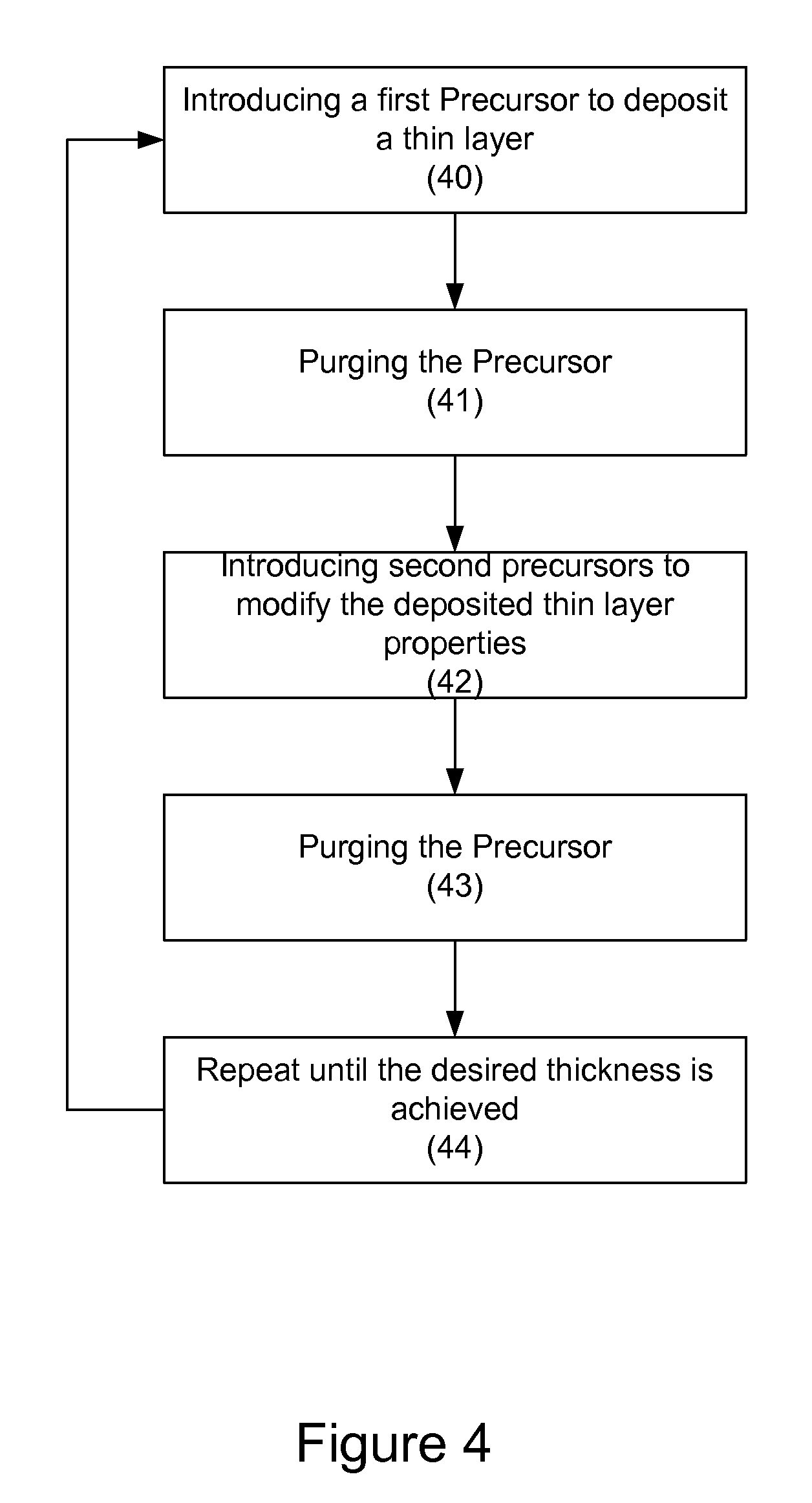
[0047]In one aspect of the invention, the present invention method to deposit a thin film on a substrate comprises the steps of:

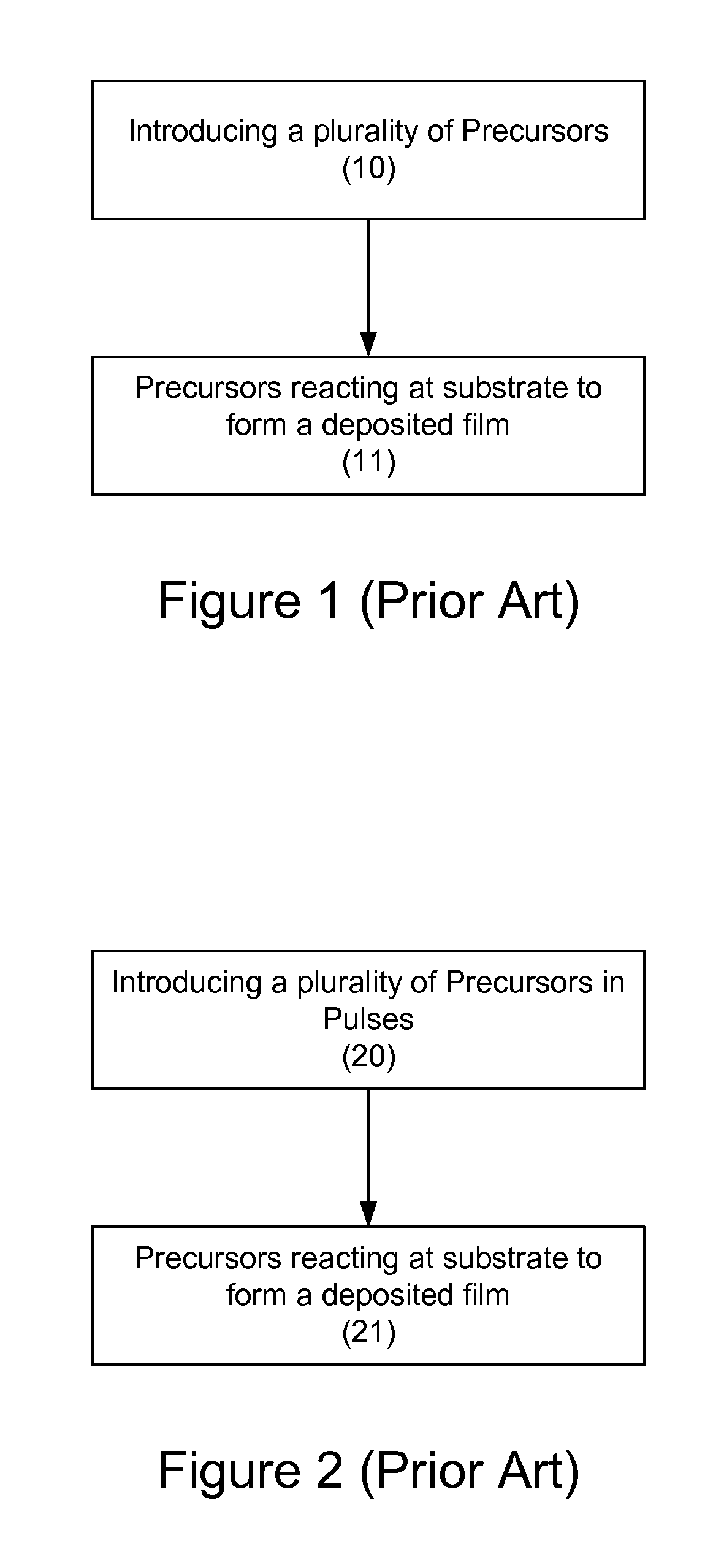
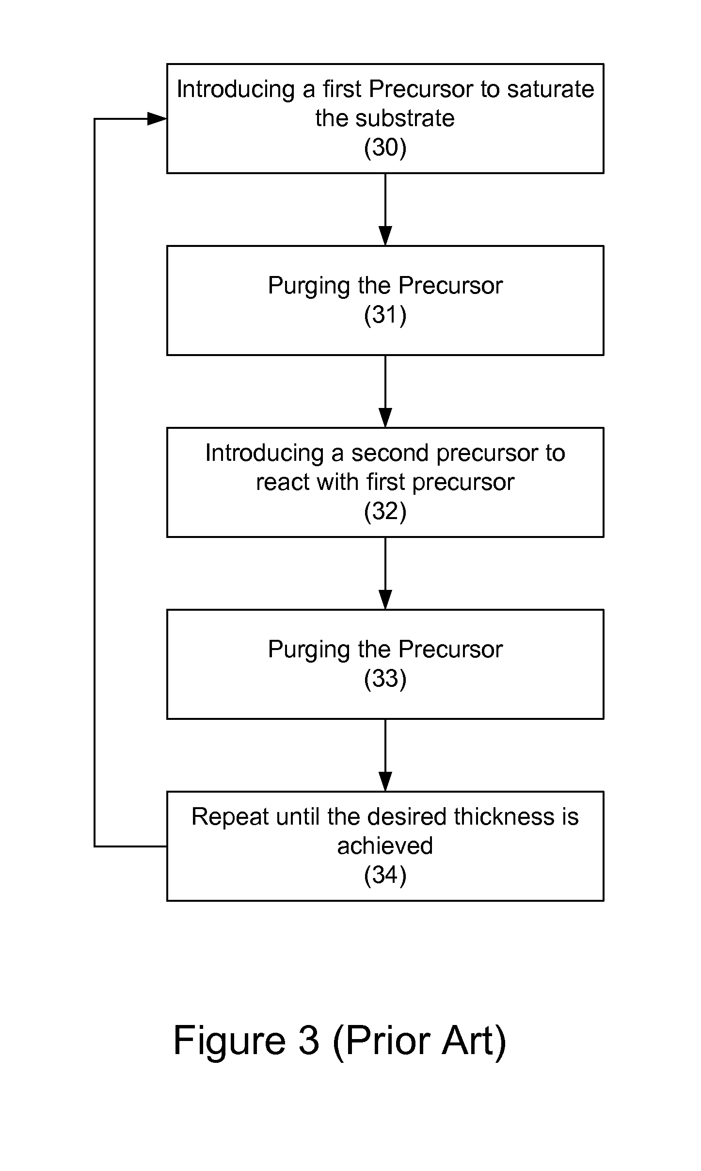
DEPOSITION STEP (a). introducing a first plurality of precursors to deposit a thin film on a substrate, the deposition process being not self-limiting;

PURGING /

[0048]REPLACEMENT STEP (b). purging the first precursors; and

TREATMENT STEP (c). introducing a second plurality of precursors to modify the deposited thin film, the second plurality of precursors having at least one precursor different from the first plurality of precurs...


PUM

PropertyMeasurementUnit
Compositionaaaaaaaaaa

Abstract

A NanoLayer Deposition (NLD) process for depositing composite films of tertiary, quaternary, pentanary, and hexary stoichiometric films is provided. The inventive deposition process is a cyclic process consisting of a sequence of thin film deposition and treatment steps to obtain a desired film stoichiometry. The deposition steps are not self-limiting as in atomic layer deposition. In one embodiment for depositing a compound oxide film, the deposition process comprises a first deposition, followed by a hydrogen-containing plasma treatment, a second deposition followed by a hydrogen-containing plasma treatment, and then a third deposition followed by a hydrogen-containing plasma and then an oxygen-containing plasma treatment to produce a stoichiometric quaternary film. The cyclic process is repeated until the desired overall film thickness is achieved. The inventive process is used to fabricate high k dielectric films, ferroelectric films, piezoelectric films, and other complex oxides.

Description

CLAIM TO PRIORITY[0001]The present invention is a continuation-in-part of U.S. patent application Ser. No. 12 / 732,825, filed Mar. 26, 2010, which is a continuation of U.S. patent application Ser. No. 10 / 360,135, filed Feb. 4, 2003, now U.S. Pat. No. 7,713,592, issued May 11, 2010, all applications and patents which are incorporated herein by reference in their entirety.BACKGROUND OF THE INVENTION[0002]The present invention relates to the deposition of a tertiary, quaternary, pentary, and hexary composite film and specifically to thin film processing and semiconductor thin film processing.[0003]Deposition is one of the basic fabrication processes of modern semiconductor device structures. Deposition techniques include Physical Vapor Deposition (PVD, or sputtering), Chemical Vapor Deposition (CVD), and numerous variations of CVD such as pulsed-CVD, sequential CVD and Atomic Layer Deposition (ALD).[0004]A PVD process uses a high vacuum apparatus and generated plasma to sputter atoms an...

Claims


Application Information

Patent Timeline
IPC IPC(8): H05H1/24
CPCC23C16/409C23C16/56C23C16/45536C23C16/45531
Inventor DITIZIO, ROBERT ANTHONYNGUYEN, TUENGUYEN, TAI DUNG
Owner ASM INTERNATIONAL
Why Eureka
Try Eureka