Conductive pattern and manufacturing method thereof

a technology of conductive pattern and manufacturing method, which is applied in the field of conductive pattern, can solve the problems of low recognition speed, high cost, and thin line width formation, and achieve the effect of fine line width and easy implementation

Active Publication Date: 2012-02-09
LG CHEM LTD
View PDF3 Cites 15 Cited by
  • Summary
  • Abstract
  • Description
  • Claims
  • Application Information

AI Technical Summary

Benefits of technology

[0012]According to exemplary embodiments of the present invention, it is possible to very economically provide a conductive pattern having a more fine line width and to form the conductive pattern having the fine line width without connection traces in a large size by using an over-etching method as compared to a known method for forming a conductive pattern. In addition, according to exemplary embodiments of the present invention, it is possible to provide a conductive pattern having a ultrafine line width that cannot be easily implemented by a known method.

Problems solved by technology

However, in the case where the conductive part is formed in the conductive pattern form, there is a limit in forming the thin line width of the conductive pattern by a known printing method, and a photolithography method uses an expensive device when forming the thin line width of the conductive pattern, such that there is a disadvantage in that a cost is high.
For example, in general, a touch screen uses an ITO-based conductive film by patterning the conductive film, but when this ITO is applied to a large area touch screen, there is a problem in that a recognition speed is low due to a RC delay by a self high resistance value.
In order to overcome this problem, many companies are developing technologies for replacing the ITO by using a printing manner, but these technologies have a disadvantage in that it is difficult to manufacture an invisible ultrafine pattern in terms of visibility.

Method used


Image

  • Conductive pattern and manufacturing method thereof
  • Conductive pattern and manufacturing method thereof
  • Conductive pattern and manufacturing method thereof

Examples


examples 2 to 7

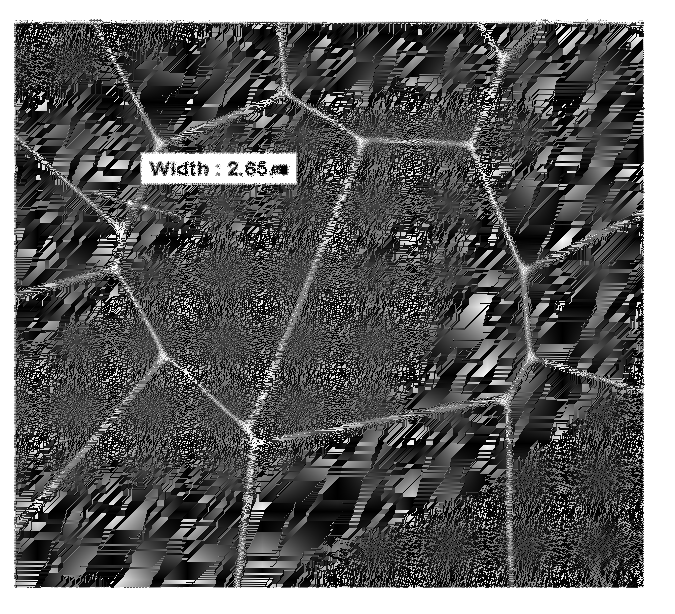
[0096]The conductive film was etched under the conditions of the just-etching time (30 sec) (Example 2), 1.3 times the just-etching time (Example 3), 1.5 times the just-etching time (Example 4), 2 times the just-etching time (Example 5), 3 times the just-etching time (Example 6), and 5 times the just-etching time (Example 7), respectively. When the film was etched 3 times the just-etching time (Example 6), the line width was 6.05 micrometers, and at this time, the picture is illustrated in FIG. 15.

[0097]Subsequently, the etching resist ink of the Bouronoi pattern was removed. The picture in which the etching resist ink is removed is illustrated in FIG. 16. The line width of each Example is described below.

TABLE 1BeforeAfter etching resist is removedetching resistExampleExampleExampleExampleExampleExampleis removed234567Line width6.055.664.964.664.464.071.59(micrometer)

example 8

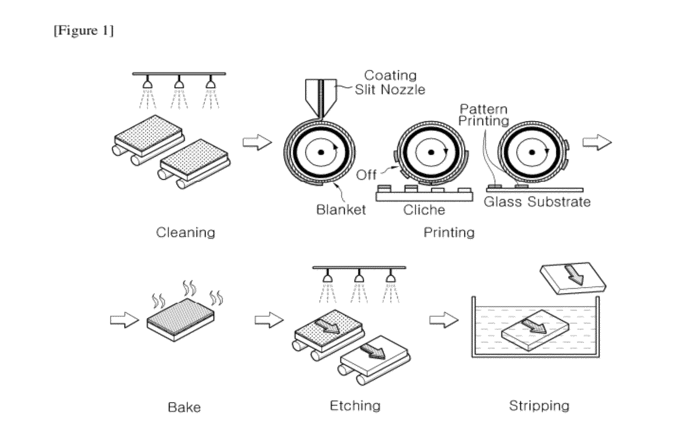
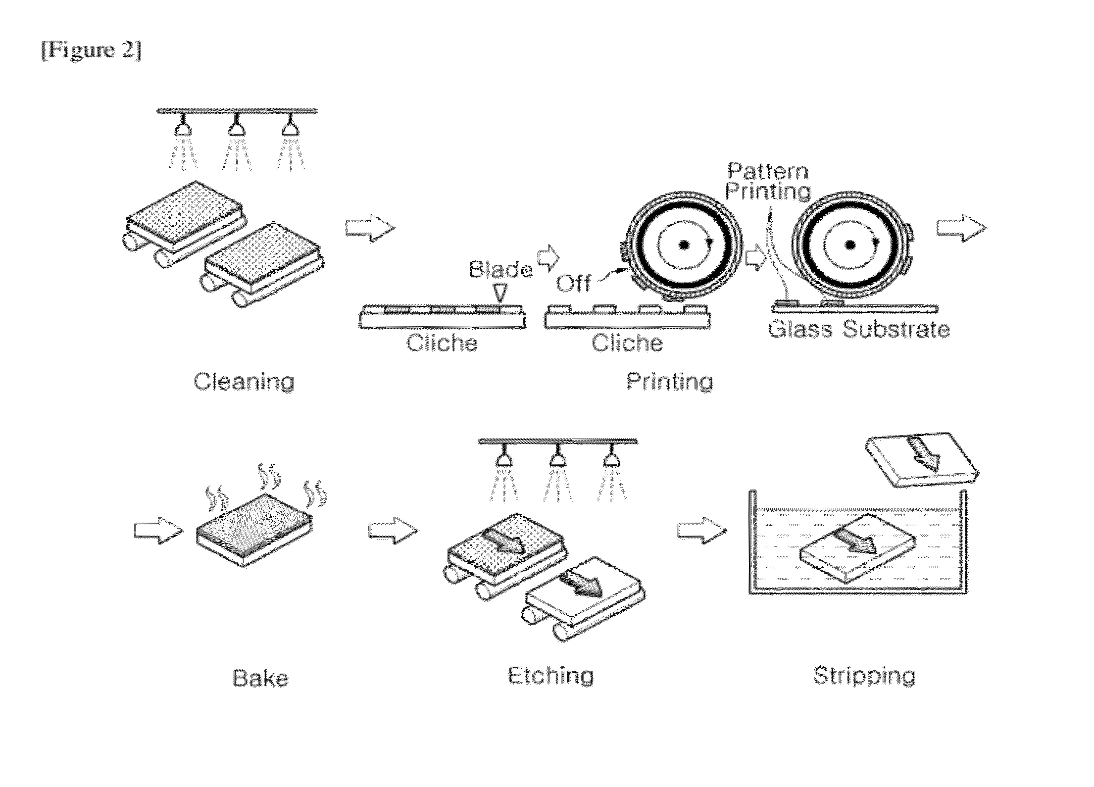
[0098]The glass substrate was manufactured by depositing the Ni metal on 0.5 t glass in the thickness of 20 nm, Ag thereon in the thickness of 200 nm, and Ni thereon in the thickness of 20 nm by the sputtering process.

[0099]Thereafter, the UV curable ink (LGP-7 manufactured by Natoco, Co., Ltd. (Japan)) was printed by using the cliché having the size of line width 8 microns / pitch 200 microns and the Bouronoi irregular pattern by using the gravure offset printing.

[0100]Thereafter, the printed sample was exposed in about 500 mJ / cm2 by the UV curing, and the bake process of the substrate was performed at 130° C. for 30 min. Subsequently, the conductive pattern having the same structure as FIG. 13 was obtained by performing the etching for about 60 sec (just etching time 20 sec) at 40° C. by using the A1 etchant (the mixed solution of the phosphoric acid, the nitric acid, the acetic acid, and water) manufactured by Zeus Co., Ltd. (Korea). Since the UV curable ink was transparent, the me...


PUM

PropertyMeasurementUnit
widthaaaaaaaaaa
widthaaaaaaaaaa
thicknessaaaaaaaaaa

Abstract

The present invention provides a method for manufacturing a conductive pattern, comprising the steps of: a) forming a conductive film on a substrate; b) forming an etching resist pattern on the conductive film; and c) forming a conductive pattern having a smaller line width than a width of the etching resist pattern by over-etching the conductive film by using the etching resist pattern, and a conductive pattern manufactured by using the same. According to the exemplary embodiment of the present invention, it is possible to effectively and economically provide a conductive pattern having a ultrafine line width.

Description

TECHNICAL FIELD [0001]The present invention relates to a conductive pattern and a method for manufacturing the same. This application claims priority from Korean Patent Application Nos. 10-2009-0009750 and 10-2009-0127756 filed on Feb. 6, 2009 and Dec. 21, 2009 in the KIPO, the disclosure of which is incorporated herein by reference in its entirety.BACKGROUND ART [0002]Conductive parts such as electrodes are used in electronic diodes such as a touch screen, a display, and a semiconductor. Currently, as transparency is needed for various electronic diodes, the conductive parts are required to have excellent conductivity and invisibility. In particular, in the touch screen, sensitivity to touch and recognition of multi-touch are required more and more, and development of the conductive parts that can implement this performance is required.[0003]The conductive parts may be formed in a conductive pattern or a transparent conductive film form. However, in the case where the conductive pa...

Claims


Application Information

Patent Timeline
Patent Type & Authority Applications(United States)
IPC IPC(8): H05K1/00H05K3/10
CPCY10T29/49156G06F3/045H05K2203/0143G06F2203/04103Y10T29/49155G03F7/40H05K2203/1184H05K3/10H05K2203/0108H05K2203/0537H05K3/0079H01L31/022425H05K2203/1105H05K2203/0571H05K1/0296Y02E10/50H05K3/061C23F1/02
Inventor HWANG, JI-YOUNGHWANG, IN-SEOKLEE, DONG-WOOKPARK, MIN-CHOONLEE, SEUNG-HEONCHUN, SANG-KISON, YONG-KOOKOO, BEOM-MO
Owner LG CHEM LTD
Why Eureka
Try Eureka