Silicon-germanium heterojunction bipolar transistor and manufacturing method of the same

a silicongermanium heterojunction and transistor technology, applied in the field of manufacturing, can solve the problems of restricting the system integration of radio frequency circuits, not realizing only achieving different breakdown voltages on the same chip, so as to increase the breakdown voltage, and increase the breakdown voltage

Inactive Publication Date: 2012-02-09
SHANGHAI HUA HONG NEC ELECTRONICS
View PDF4 Cites 11 Cited by
  • Summary
  • Abstract
  • Description
  • Claims
  • Application Information

AI Technical Summary

Benefits of technology

[0049]1. The present invention drastically increases the breakdown voltage of the SiGe HBT because the pseudo buried layer is used to replace the N-type buried layer (NBL) in the SiGe HBT in the prior art, which greatly increases the breakdown voltage of the BC junction, that is the breakdown voltage of PN junction formed between the base region and the collector region, and also makes the breakdown of BC junction determined by the lateral depletion region instead of the vertical depletion region. The lateral BC junction depletion region may stop in the pseudo buried layers, so the size of the collector region that extends laterally into the bottom of the field oxide regions will determine the breakdown voltage of the BC junction and then determine the breakdown voltage (BVCEO) of the SiGe HBT. Therefore, the present invention increases the breakdown voltage of the BC junction of devices and the breakdown voltage (BVCEO) of the SiGe HBT through increasing the size of a collector region which extends laterally into field oxide regions.
[0050]2. The present invention is favorable for the SiGe HBT devices with different voltages to integrate on the same chip. Because, with the structure of the SiGe HBT devices in the present invention, the breakdown voltage of the SiGe HBT devices can be adjusted conveniently only by changing the size of the collector region that extends laterally into the bottom of the field oxide regions. Therefore, without changing the process conditions of devices, the present invention can produce serial high-voltage SiGe HBT devices with different breakdown voltages on the same chip only by changing of the layout. Therefore, the integration of the SiGe HBT devices with different breakdown voltages can be realized. At the same time, the integration of devices in the present invention does not need the change of the process conditions of the devices, that is, the depth and dosage concentration of the collector region are not changed, so the equivalent resistance and the BC junction capacitance in the collector region will not show a large degree of change, thus the cutoff frequency will remain relatively stable.
[0051]3. The present invention can also reduce the size of devices. The SiGe HBT in the present invention adopts a deep-hole contact to pick up the pseudo buried layer as the collector, so the problem of a too large area of the devices caused by adopting N-sinker for the existing SiGe HBT is avoided, and at the same time, the parasitic resistance of the collector is also reduced.

Problems solved by technology

Therefore, traditional high-voltage SiGe HBTs could only achieve different breakdown voltages by change of process.
SiGe HBTs that can not realize different breakdown voltages on the same chip restrict the system integration of radio frequency circuits.

Method used


Image

  • Silicon-germanium heterojunction bipolar transistor and manufacturing method of the same
  • Silicon-germanium heterojunction bipolar transistor and manufacturing method of the same
  • Silicon-germanium heterojunction bipolar transistor and manufacturing method of the same

Examples


Embodiment Construction

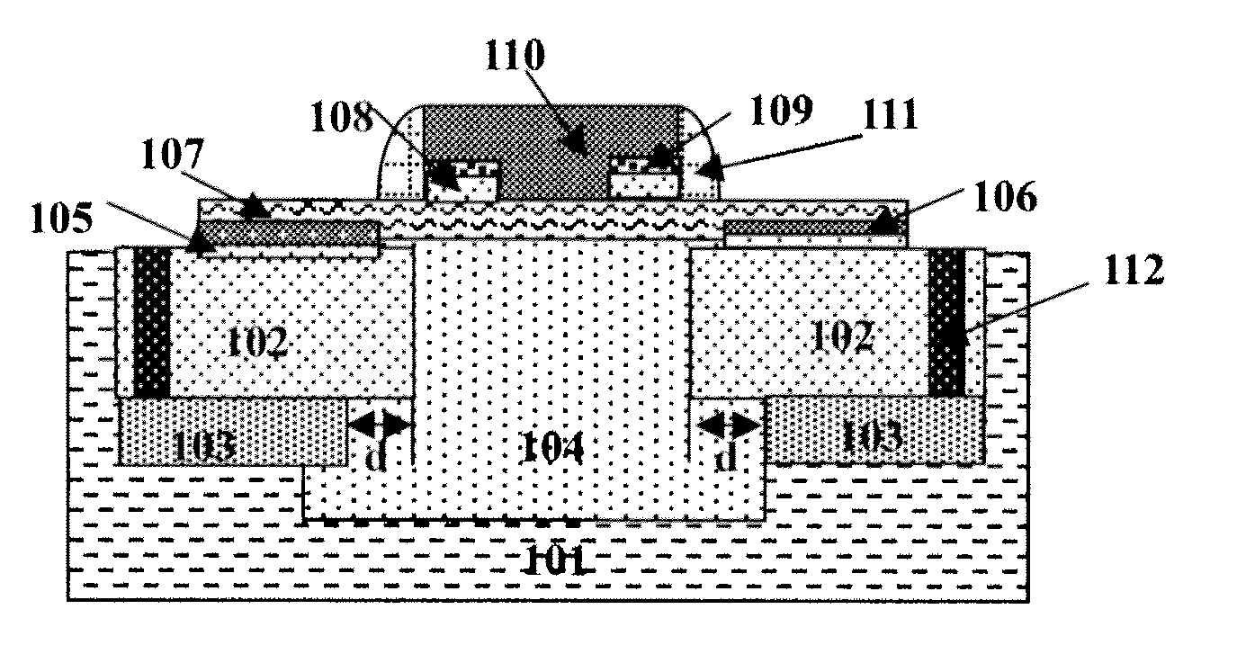
[0055]As is shown in FIG. 1, it is a structure diagram of the Silicon-Germanium heterojunction bipolar transistor(SiGe HBT) in the embodiment of the present invention. The SiGe HBT in the embodiment of the present invention is formed on a P-type silicon substrate 101, and an active region is isolated by field oxide regions 102. The SiGe HBT includes:

[0056]A collector region 104, consisting of an N-type ion implantation region formed in the active region, wherein the collector region 104 is deeper than the bottom of the field oxide regions 102, and the collector region 104 extends laterally into the bottom of the field oxide regions 102 on both sides of the active region. The process conditions of the N-type ion implantation of the collector region 104 are: the implantation dose is 1 e12 cm−2˜5 e14 cm−2 and the implantation energy is 50 KeV˜500 KeV.

[0057]Pseudo buried layers 103, each consisting of an N-type ion implantation region and respectively formed at the bottom of the field o...


PUM


Abstract

A Silicon-Germanium heterojunction bipolar transistor (SiGe HBT) formed on a silicon substrate, wherein, an active region is isolated by field oxide regions, a collector region is formed in the active region and extends into the bottom of the field oxide regions; pseudo buried layers are formed at the bottom of the field oxide regions. Each of the pseudo buried layers is a lateral distance away from the active region and contacts with a part of the collector region. Deep-hole contacts are formed in the field oxide regions located on top of the pseudo buried layers to pick up the collector region. The present invention can adjust the breakdown voltage of devices through adjusting the lateral distance. A method for manufacturing the SiGe HBT is also disclosed.

Description

CROSS-REFERENCES TO RELATED APPLICATIONS[0001]This application claims the priority of Chinese patent application number 201010245833.6, filed on Aug. 5, 2010, the entire contents of which are incorporated herein by reference.BACKGROUND OF THE INVENTION[0002]1. Field of the Invention[0003]The present invention relates to the manufacturing field of semiconductor integrated circuits and, more particularly, to a Silicon-Germanium heterojunction bipolar transistor(SiGe HBT). The present invention also relates to a manufacturing method of SiGe HBT.[0004]2. Description of Related Art[0005]With the growing maturity of Silicon-Germanium (SiGe) process, radio frequency circuit integration is becoming more and more popular. The radio frequency receiving, radio frequency emission and switching, etc. are all tending toward integration, so the low noise amplifier (LNA) for amplifying received signals and the power amplifier (PA) for amplifying emitted signals shall be fabricated on the same chip....

Claims


Application Information

Patent Timeline
Patent Type & Authority Applications(United States)
IPC IPC(8): H01L29/70H01L21/331
CPCH01L29/0649H01L29/7378H01L29/66242H01L29/0821
Inventor QIAN, WENSHENG
Owner SHANGHAI HUA HONG NEC ELECTRONICS
Why Eureka
Try Eureka