Process for producing organic electroluminescence element, organic electroluminescence element, organic el display, and organic el lighting

Inactive Publication Date: 2012-02-16
MITSUBISHI CHEM CORP
12 Cites 18 Cited by

AI-Extracted Technical Summary

Problems solved by technology

However, this vacuum deposition method is unsuitable for the production of large displays or surface-emitting lightings having a large area because deposition of a homogeneous film on a substrate having a large...

Method used

[0060]Groups which undergo a cyclization addition reaction, such as arylvinylcarbonyl groups, e.g., cinnamoyl, and groups derived from a benzocyclobutene ring, are preferred from the standpoint of further improving electrochemical stability.
[0106]The composition for luminescent-layer formation in the invention may contain various additives such as a leveling agent and an antifoamer so as to have improved film-forming properties.
[0131]Namely, it is presumed that the arylamine compound is inhibited from becoming a radical cation by blocking light having wavelengths shorter than 500 nm and, as a result, excitons in the luminescent layer are prevented from being deactivated. Consequently, according to the invention, excitons which contribute to luminescence are available in a larger amount, and the luminance is improved.
[0137]The substrate 1 serves as the support of the organic electroluminescence element, and use may be made of a plate of quartz or glass, a metal plate, a metal foil, a plastic film or sheet, or the like. Especially preferred are a glass plate and a plate of a transparent synthetic resin such as a polyester, polymethacrylate, polycarbonate, or polysulfone. In the case of using a synthetic-resin substrate, it is necessary to take account of gas barrier properties. In case where the substrate has too low gas barrier properties, there are cases where the surrounding air might pass through the substrate to deteriorate the organic electroluminescence element. Too low gas barrier properties are hence undesirable. Consequently, one of preferred methods is to form a dense silicon oxide film on at least one surface of a synthetic-resin substrate to ensure gas barrier properties.
[0143]It is preferred that the surface of the anode 2 should be subjected to an ultraviolet (UV)/ozone treatment or a treatment with an oxygen plasma or argon plasma for the purposes of removing impurities adherent to the anode 2 and regulating ionization potential to improve hole injection properties.
[0164]These electron-accepting compounds oxidize the hole-transporting compound and can thereby improve the conductivity of the hole injection layer.
[0242]The electron transport ...

Benefits of technology

[0012]According to the invention, the organic electroluminescence element, which has a luminescent layer containing an arylamine compound and formed by a wet film formation method, has a high luminescence and a long working life.
[0013]According t...

Abstract

An organic electroluminescence element having a long working life, which has a luminescent layer containing an arylamine compound and formed by a wet film formation method, and an organic EL display and an organic EL lighting which each are equipped with the electroluminescence element. In addition, a process for producing an organic electroluminescence element having a long working life, which has a luminescent layer containing an arylamine compound and formed by a wet film formation method. The organic electroluminescence element contains a first electrode, a second electrode formed so as to be opposed to the first electrode, and a luminescent layer disposed between the first electrode and the second electrode, where the luminescent layer contains an arylamine compound, and the luminescent layer was formed by a wet film formation in an environment shielded from light having a wavelength shorter than 500 nm.

Application Domain

Electroluminescent light sourcesSolid-state devices +6

Technology Topic

Organic electroluminescenceChemistry +3

Image

  • Process for producing organic electroluminescence element, organic electroluminescence element, organic el display, and organic el lighting
  • Process for producing organic electroluminescence element, organic electroluminescence element, organic el display, and organic el lighting
  • Process for producing organic electroluminescence element, organic electroluminescence element, organic el display, and organic el lighting

Examples

  • Experimental program(18)

Example

Reference Example 1
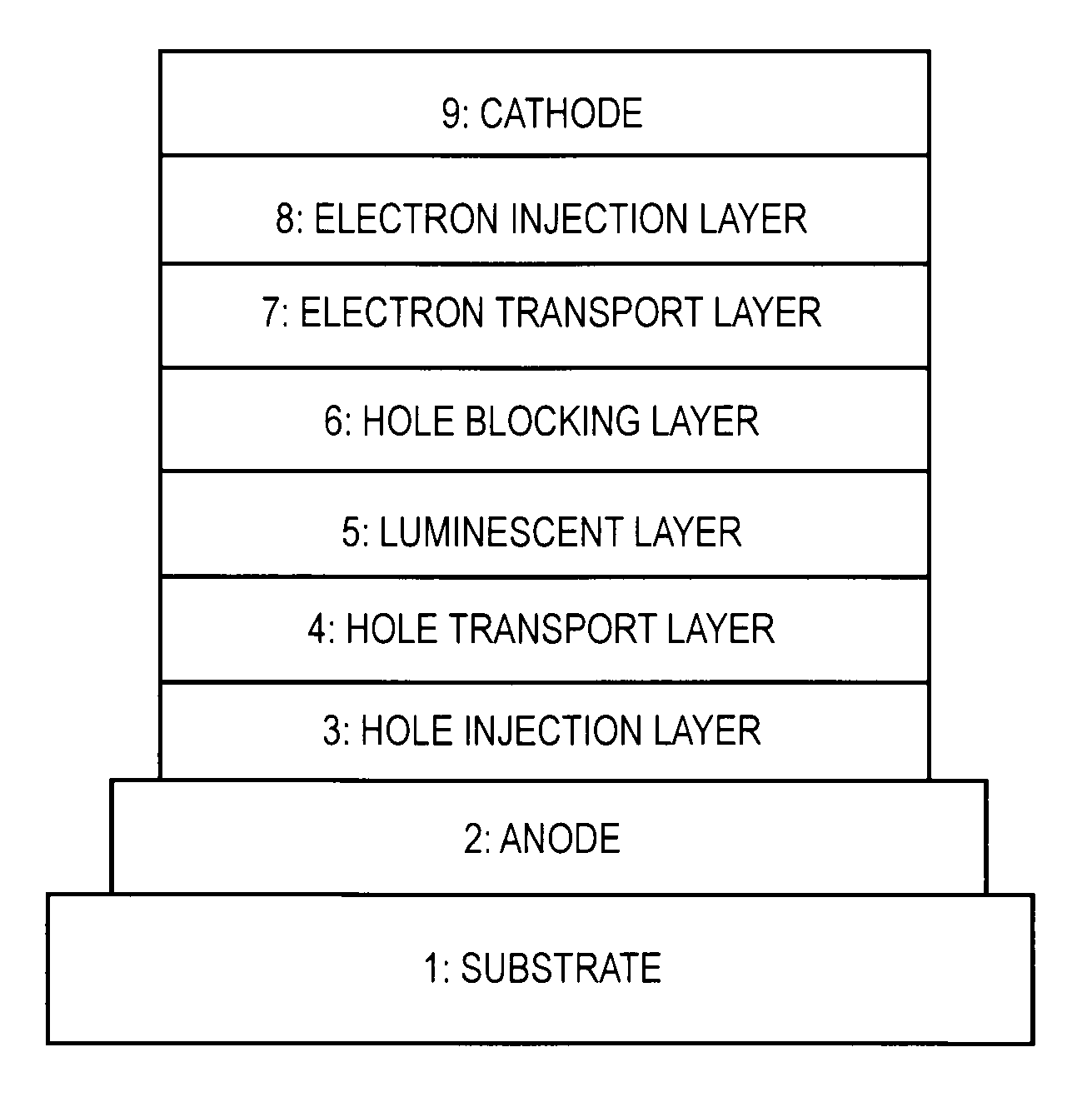
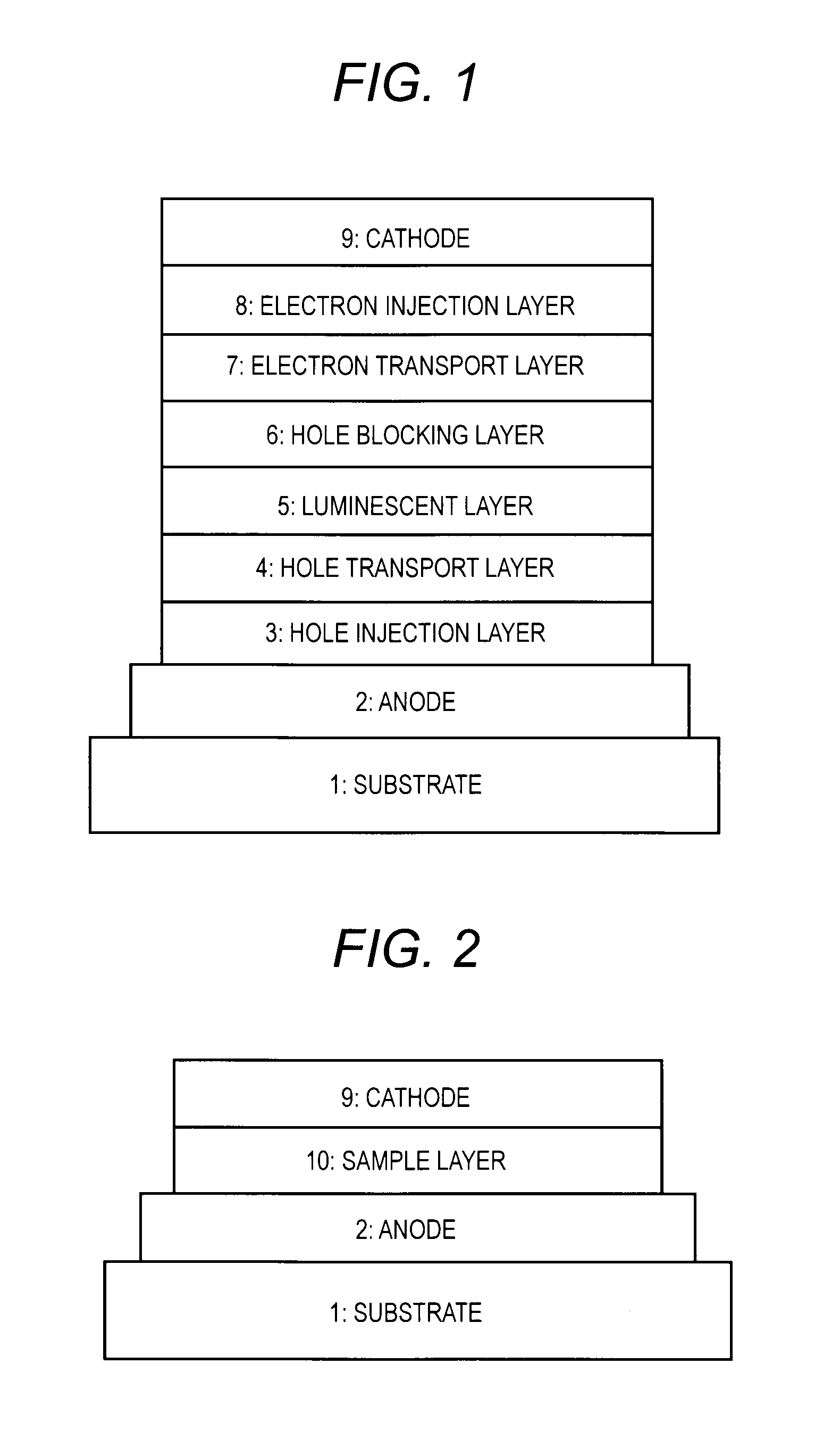
[0272]An element for dielectric constant measurement which had the structure shown in FIG. 2 was produced. A substrate constituted of a glass substrate and, formed thereon, a transparent conductive film of indium-tin oxide (ITO) deposited in a thickness of 70 nm (deposited by sputtering; manufactured by Sanyo Vacuum Industries Co., Ltd.) was subjected to processing by an ordinary technique of photolithography and etching with hydrochloric acid to pattern the transparent conductive film into stripes having a width of 2 mm. Thus, an anode 2 was formed. The ITO substrate which had undergone the patterning was cleaned by subjecting the substrate to ultrasonic cleaning with an aqueous surfactant solution, rinsing with ultrapure water, ultrasonic cleaning with ultrapure water, and rinsing with ultrapure water in this order, subsequently dried with compressed air, and finally subjected to ultraviolet/ozone cleaning. This ITO functions as an electrode.
[0273]A coating fluid containing compound (C1), arylamine compound (C2), and compound (D1) respectively represented by the following structural formulae was prepared. The coating fluid was applied to the substrate having patterned ITO by spin coating and heated, under the following conditions in an environment having the spectrum shown in FIG. 3. Thus, a sample layer 10 was formed. This sample layer had a thickness of 206 nm.
[0274]Solvent toluene
[0275]Coating fluid concentrations [0276] C1: 0.75 wt % [0277] C2: 2.25 wt % [0278] D1: 0.30 wt %
10
[0279]
Spinner rotation speed 500 rpm Spinner rotation period 30 sec Spin coating atmosphere in nitrogen Heating conditions 130° C.; 1 hr; in nitrogen
[0280]Here, the substrate was transferred to a vacuum deposition apparatus. A shadow mask in the form of stripes with a width of 2 mm was brought, as a mask for counter-electrode deposition, into close contact with the element so that these stripes were perpendicular to the ITO stripes of the electrode 2. The apparatus was evacuated until the degree of vacuum within the apparatus became at least 5.0×10⁻⁴ Pa.
[0281]Aluminum was heated using a molybdenum boat in the same manner to form an aluminum layer having a thickness of 80 nm as a counter electrode 9 while regulating the rate of deposition so as to be in the range of 1.0-10.0 Å/sec.
[0282]Subsequently, sealing was conducted in the following manner in order to prevent the element from being deteriorated by the action of atmospheric moisture, etc. during storage.
[0283]In a gloved nitrogen box, a photocurable resin (30Y-437, manufactured by ThreeBond Co., Ltd.) was applied in a width of about 1 mm to the periphery of a glass plate having a size of 23 mm×23 mm, and a moisture getter sheet (manufactured by Dynic Corp.) was disposed in a central part. The substrate on which the cathode had been formed was laminated to the getter sheet so that the side having the deposited layers faced the desiccant sheet. Thereafter, only the region where the photocurable resin had been applied was irradiated with ultraviolet light to cure the resin.
[0284]Thus, an element for dielectric constant measurement which had an area with a size of 2 mm×2 mm was obtained. This element was examined with dielectric analysis system Model SI 126096W, manufactured by Solartron, while applying an alternating-current voltage of 100 mV thereto at 0.1 Hz to 10 kHz.
[0285]The values of dielectric constant obtained are shown in Table 1.

Example

Reference Example 2
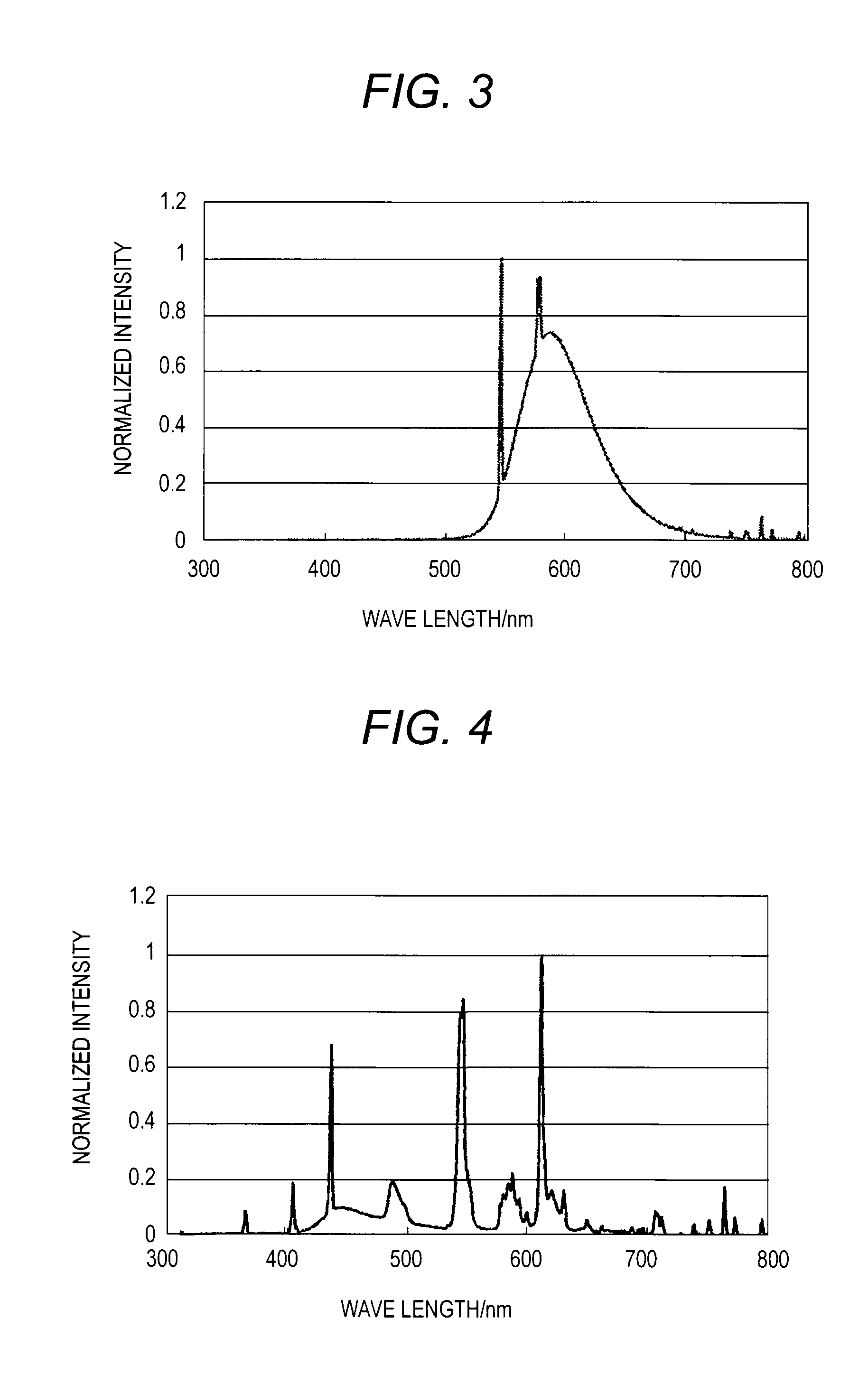
[0286]An element for dielectric constant measurement was produced in the same manner as in Reference Example 1, except that a sample layer 10 was formed in an environment having the spectrum shown in FIG. 4.
[0287]The values of dielectric constant obtained are shown in Table 1.

Example

Reference Example 3
[0288]An element for dielectric constant measurement was produced in the same manner as in Reference Example 1, except that a sample layer 10 having a thickness of 232 nm was formed by preparing a coating fluid containing compound (C3) and arylamine compound (D2) respectively represented by the following structural formulae and subjecting the coating fluid to application by spin coating and heating in an environment having the spectrum shown in FIG. 3.
[0289]Solvent toluene
[0290]Coating fluid concentrations [0291] C3: 3.0 wt % [0292] D2: 0.3 wt %
10
[0293]
Spinner rotation speed 500 rpm Spinner rotation period 30 sec Spin coating atmosphere in nitrogen Heating conditions 130° C.; 1 hr; in nitrogen
[0294]The values of dielectric constant obtained are shown in Table 1.

PUM

PropertyMeasurementUnit
Wavelength500.0nm
Temperature1.0°C
Length4.572E-5 ~ 1.016E-4m

Description & Claims & Application Information

We can also present the details of the Description, Claims and Application information to help users get a comprehensive understanding of the technical details of the patent, such as background art, summary of invention, brief description of drawings, description of embodiments, and other original content. On the other hand, users can also determine the specific scope of protection of the technology through the list of claims; as well as understand the changes in the life cycle of the technology with the presentation of the patent timeline. Login to view more.

Similar technology patents

High-brightness luminescent yarn and manufacturing method thereof

ActiveUS20200347524A1high luminancelong life time
Owner:CHANCE LINE IND

Display control device and method of controlling display device

ActiveUS20200410930A1high luminance
Owner:LG DISPLAY CO LTD

Light emitting element and iridium complex

ActiveUS7303826B2high luminancehigh efficiency
Owner:UDC IRELAND +1

Organic electron transport material

InactiveUS20180358561A1high luminancelong device life
Owner:GUANGDONG AGLAIA OPTOELECTRONICS MATERIALS +1

Classification and recommendation of technical efficacy words

  • high luminance
  • long work life

Light source unit and projector

ActiveUS20090262308A1high luminance
Owner:CASIO COMPUTER CO LTD

Liquid crystal display

InactiveUS20060243948A1excellent cooling functionhigh luminance
Owner:SHARP KK

Flat light source device

InactiveUS20050248960A1high luminance
Owner:MITSUBISHI RAYON CO LTD

Luminance-enhancing film, optical sheet member, and liquid crystal display device

ActiveUS20160170114A1high luminancesuppress change of color
Owner:FUJIFILM CORP

Backlight unit and liquid crystal display device having the same

ActiveUS20060146570A1high luminancehigh color reproduction
Owner:LG DISPLAY CO LTD

Testing head comprising vertical probes

InactiveUS20170122983A1long work life
Owner:TECHNOPROBE
Why Eureka
Try Eureka