Plasma Deposition of Amorphous Semiconductors at Microwave Frequencies

a technology of amorphous semiconductors and microwave frequencies, applied in the field of plasma chemistry and physics, can solve the problems of preventing or slowing down the relaxation or decay of solar energy on a scale sufficient to meaningfully reduce fossil fuel consumption, and achieve the effects of maximizing the concentration of fluorine, preventing or slowing down the relaxation or decay, and increasing the porosity of product films

Inactive Publication Date: 2012-02-16
OVSHINSKY TECH
View PDF33 Cites 82 Cited by
  • Summary
  • Abstract
  • Description
  • Claims
  • Application Information

AI Technical Summary

Benefits of technology

[0034]The deposition chamber may also include a supplemental energizing source to prevent or slow relaxation or decay of the energized species entering the deposition chamber from one or more conduits of the microwave applicator. The supplemental energy source can also be used to activate species in the deposition chamber to form intermediate species through bond cleavage. The presence of fluorine, for example, can be increased by activating SiF4 to cleave an Si—F bond to liberate fluorine. In one embodiment, the supplemental energy source is an electromagnetic source that includes an antenna array. The antenna array may generate or sustain an electromagnetic field and may further provide phase control. In one embodiment, the electromagnetic field is a microwave field.
[0035]The deposition chamber is further equipped with means to meter, monitor, modulate and calibrate the presence and distribution of species in the growth ambient. This capability permits fine control over the ratios of the multiple elements in deposition environment to ins

Problems solved by technology

Implementation of solar energy on a scale sufficient to meaningfully reduce fossil

Method used


Image

  • Plasma Deposition of Amorphous Semiconductors at Microwave Frequencies
  • Plasma Deposition of Amorphous Semiconductors at Microwave Frequencies
  • Plasma Deposition of Amorphous Semiconductors at Microwave Frequencies

Examples


example 1

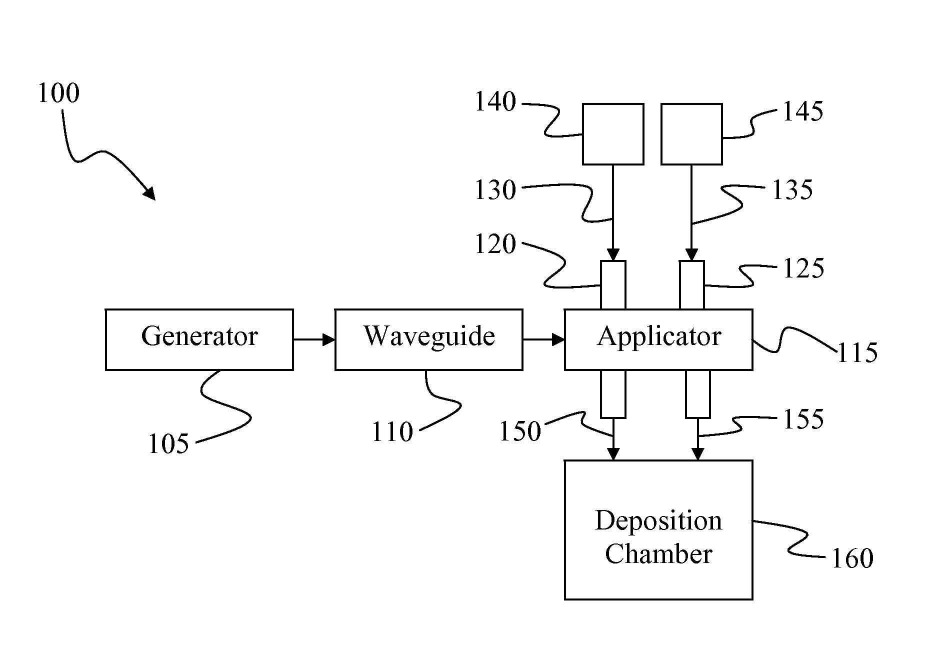
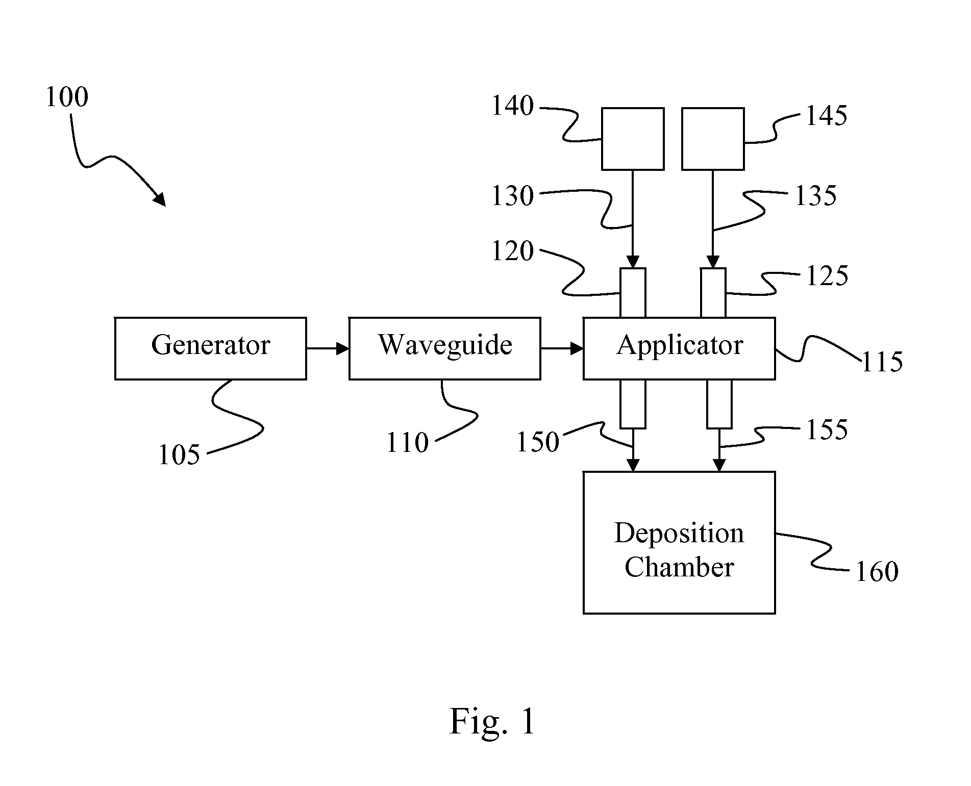
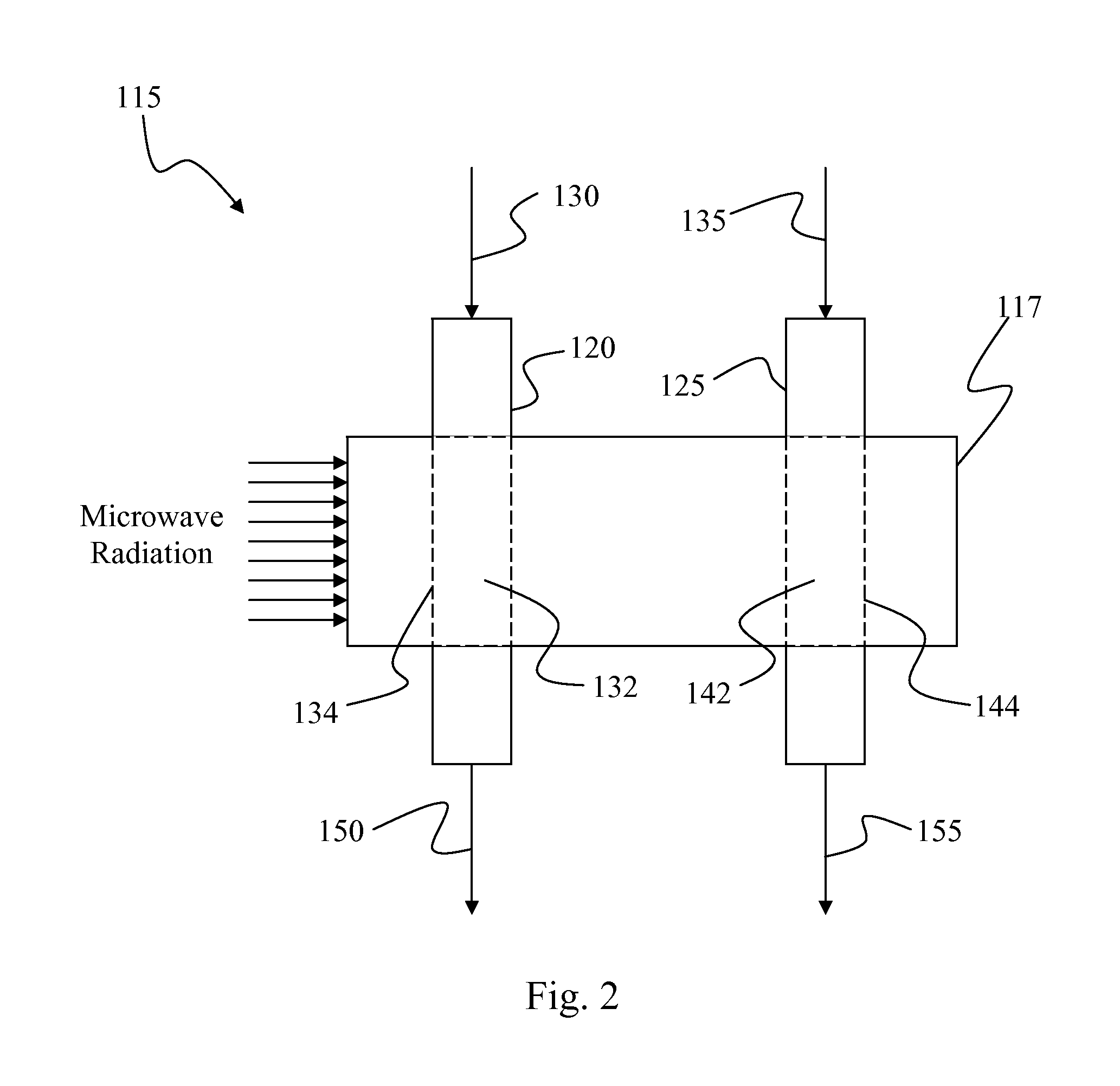
[0084]In this example, selected compositional and optical absorption characteristics of representative thin film materials comprising amorphous silicon in accordance with the instant invention are described. The materials are denominated Sample 547 and Sample 548 and were prepared in a deposition system similar to that shown in FIG. 4 that included a single microwave applicator with a single conduit passing therethrough and a single supplemental inlet for delivering a non-energized supplemental material stream. The conduit was made from sapphire and the substrate was positioned about 4 inches from the interface of the conduit with the deposition chamber. A mixture of 1 standard liter per minute of SiF4 and 2 standard liters per minute of argon was introduced to the conduit of the microwave applicator and activated with microwave radiation at a frequency of 2.45 GHz and a power of 600 W. SiH4 was introduced at a rate of 1 standard liter per minute to the deposition chamber through th...

example 2

[0099]In this example, the effect of process gas ratio on the deposition rate and photoconductivity of representative materials comprising amorphous silicon in accordance with the instant invention is described. The samples were prepared using the deposition system described in Example 1 hereinabove. A mixture of 1 standard liter per minute of SiF4 and 2 standard liters per minute of argon was introduced to the conduit of the microwave applicator and activated with microwave radiation at a frequency of 2.45 GHz and a power of 600 W. Instead of SiH4, however, disilane (Si2H6) was introduced to the deposition chamber through the supplemental delivery port and delivered as an electrically-neutral material stream. The flow rate of disilane was systematically adjusted to provide a series of samples for which the ratio of the flow rate of disilane to the ratio of the flow rate of SiF4 ranged from 0.3 to 2.0. The energized stream of SiF4 and argon exiting the conduit of the microwave appli...

example 3

[0104]In this example, the effect of substrate temperature on the deposition rate and photoconductivity of representative materials comprising amorphous silicon in accordance with the instant invention is described. The samples were prepared using the deposition system described in Example 1 hereinabove. A mixture of 1 standard liter per minute of SiF4 and 2 standard liters per minute of argon was introduced to the conduit of the microwave applicator and activated with microwave radiation at a frequency of 2.45 GHz and a power of 600 W. Instead of SiH4, however, disilane (Si2H6) was introduced at a rate of 1 standard liter per minute to the deposition chamber through the supplemental delivery port. The disilane was delivered in an electrically-neutral state. The Si2H6 / SiF4 flow rate ratio was fixed at 1.0 in these experiments. The energized stream of SiF4 and argon exiting the conduit of the microwave applicator and the non-energized stream of disilane supplied by the supplemental d...


PUM

PropertyMeasurementUnit
Poweraaaaaaaaaa
Concentrationaaaaaaaaaa
Energyaaaaaaaaaa

Abstract

Apparatus and method for plasma deposition of thin film photovoltaic materials at microwave frequencies. The apparatus avoids unintended deposition on windows or other microwave transmission elements that couple microwave energy to deposition species. The apparatus includes a microwave applicator with conduits passing therethrough that carry deposition species. The applicator transfers microwave energy to the deposition species to activate or energize them to a reactive state conducive to formation of a thin film material. The conduits physically isolate deposition species that would react or otherwise combine to form a thin film material at the point of microwave power transfer. The deposition species are separately energized and swept away from the point of power transfer to prevent thin film deposition. Suitable deposition species include precursors that contain silicon, germanium, fluorine, and/or hydrogen. The invention allows for the ultrafast formation of silicon-containing amorphous semiconductors that exhibit high mobility, low porosity, little or no Staebler-Wronski degradation, and low defect concentration.

Description

FIELD OF INVENTION[0001]The invention establishes a new realm of plasma chemistry and physics that enables the deposition of unique atomically-engineered multi-element compositions for photovoltaic applications that free the world from its dependence on fossil fuels. More particularly, this invention solves the problem of depositing silicon-containing semiconductors at high deposition rates to achieve highly efficient photovoltaic materials with a low density of states that exhibit no Staebler-Wronski degradation. Most particularly, this invention relates to plasma deposition of amorphous, nanocrystalline, microcrystalline, polycrystalline or single crystalline semiconductors at microwave frequencies from multiple source gases, one of which includes fluorine, in a process that avoids undesirable coatings on microwave windows.BACKGROUND OF THE INVENTION[0002]Concern over the depletion and environmental impact of fossil fuels has stimulated strong interest in the development of altern...

Claims


Application Information

Patent Timeline
IPC IPC(8): H01L31/18
CPCC23C16/24Y02E10/547H01J37/32211H01J37/3244H01J37/32477H01J37/3277H01L21/02532H01L21/02592H01L21/0262H01L31/028H01L31/03767H01L31/065H01L31/076H01L31/202H01L31/204Y02E10/548C23C16/452Y02P70/50
Inventor OVSHINSKY, STANFORD R.STRAND, DAVIDKLERSY, PATRICKPASHMAKOV, BOIL
Owner OVSHINSKY TECH
Why Eureka
Try Eureka