Photonic crystal slot waveguide miniature on-chip absorption spectrometer

a technology of optical spectroscopy and crystal slot, which is applied in the field of optical and medical devices, can solve the problems of inability to integrate cavity ringdown spectroscopy on-chip, inability to precisely identify analyte through spectroscopic signature, and inability to integrate on-chip, etc., and achieve enhanced optical field, enhanced light absorption, and high efficiency

Active Publication Date: 2012-02-23
OMEGA OPTICS
View PDF0 Cites 22 Cited by
  • Summary
  • Abstract
  • Description
  • Claims
  • Application Information

AI Technical Summary

Benefits of technology

[0010]The primary objective of the invention is to provide an on-chip integrated photonic crystal slot waveguide absorption spectrometer with compact size that can be monolithically integrated with lasers and detectors for the spectroscopic identification with unique absorption signatures of solid, liquids, and gases.
[0011]The second objective of the invention is to enable an on-chip analyte sampling cell determined by the slot dimensions in the photonic crystal slot waveguide, which enhances the optical absorption between the analyte and light over a given geometrical length on a chip, thereby eliminating the need for multiple pass absorption cells and complex optical elements employed in off-chip analyte sampling cells.
[0012]The third objective of the invention is to significantly increase the number of analytes that can be measured on an integrated chip level. Contemporary systems for measuring gases by cavity ring-down spectroscopy can measure up to 16 gases. However, the corresponding equipment can weigh approximately 100 pounds and occupy about 3 cubic feet of space. Since the present invention considers on-chip integration of photonic crystal slot waveguides that occupy less than 0.2 mm2 each, dense integration of waveguides can cover the entire wavelength spectrum from the near-infrared to the far-infrared on the same silicon chip.

Problems solved by technology

However, exact identification of analyte through spectroscopic signatures has not been demonstrated.
Cavity ringdown spectroscopy cannot be integrated on-chip primarily due to the stringent requirement of optical source and high finesse optical cavities for analyte sampling.
Technically, tunable diode laser absorption spectroscopy could be integrated on-chip, but the analyte sampling volume required is of the order of meters and cannot therefore be integrated on a chip.
Hence tunable diode laser absorption spectroscopy is also not a convenient method to integrate on-chip.
Furthermore, both cavity ringdown spectroscopy, due to the requirement of femtosecond lasers and high finesse optical cavities for high sensitivity, and tunable diode laser absorption spectroscopy, are very expensive, of the order of tens of thousands of dollars.
A primary drawback of both cavity ringdown spectroscopy and tunable diode laser absorption spectroscopy is the weight, size, as well as cost which significantly increases the cost of ownership of the corresponding products.
The same drawbacks of size, weight and cost hold for Fourier transform infrared spectroscopy and photoacoustic spectroscopy.
However, these devices are limited by resolution of spectrometry.
Spectrometer techniques such as cavity ring-down spectroscopy, ring resonator optical cavity, and photonic crystal cavity are limited in resolution, by the finesse of the optical cavity and the size and weight of the optical cavity.

Method used


Image

  • Photonic crystal slot waveguide miniature on-chip absorption spectrometer
  • Photonic crystal slot waveguide miniature on-chip absorption spectrometer
  • Photonic crystal slot waveguide miniature on-chip absorption spectrometer

Examples


Embodiment Construction

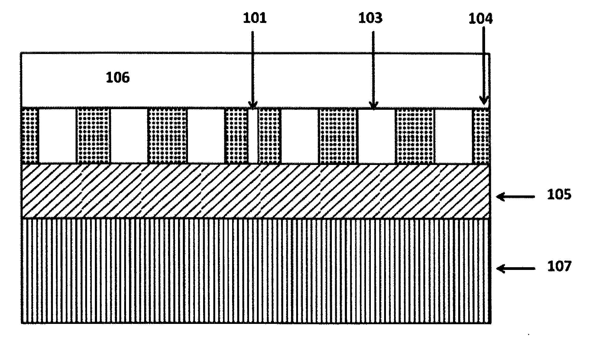
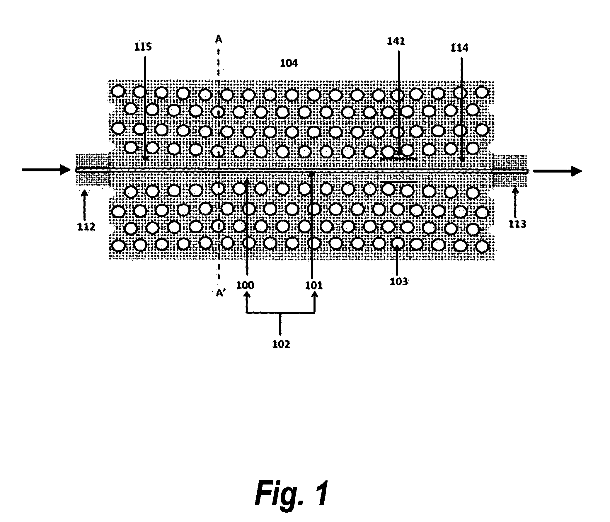
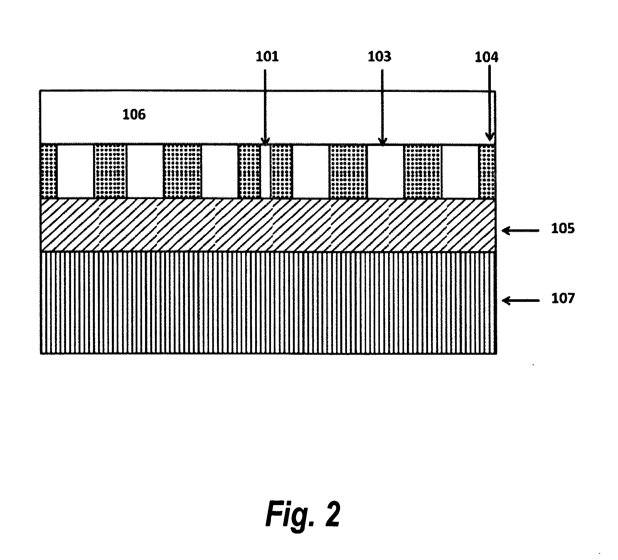
[0015]In accordance with a preferred embodiment of the present invention, a device for an on-chip integrated optical absorption spectroscopy comprises: a functional photonic crystal waveguide having a waveguide core along which light is guided, a slot at the center of the photonic crystal waveguide along the length of the photonic crystal waveguide, an input and output photonic crystal waveguide with gradually changed group index before and after the functional photonic crystal waveguide, which can bridge the refractive indices difference between conventional optical waveguides and the functional photonic crystal waveguide. The sensor can be used to detect organic or inorganic substances that can be solids and liquids. Light (from a broadband source or LED) coupled into a photonic crystal slot waveguide, in the presence of the analyte, has enhanced absorption by the analyte due to the increase in the effective optical path length caused by the enhanced field intensity in the slot an...


PUM


Abstract

Methods and systems for label-free on-chip optical absorption spectrometer consisting of a photonic crystal slot waveguide are disclosed. The invention comprises an on-chip integrated optical absorption spectroscopy device that combines the slow light effect in photonic crystal waveguide and optical field enhancement in a slot waveguide and enables detection and identification of multiple analytes to be performed simultaneously using optical absorption techniques leading to a device for chemical and biological sensing, trace detection, and identification via unique analyte absorption spectral signatures. Other embodiments are described and claimed.

Description

STATEMENT REGARDING FEDERALLY SPONSORED RESEARCH[0001]The U.S. Government has a paid-up license in this invention and the right in limited circumstances to require the patent owner to license others on reasonable terms as provided for by the terms of the contract EP-D-10-047 awarded by Environmental Protection Agency.BACKGROUND OF THE INVENTION[0002]1. Field of the Invention[0003]This invention relates generally to the field of optical and medical devices, and more specifically to an apparatus and method for on-chip optical spectroscopy for the detection and identification by unique spectral signatures of solid, liquid, or gas substances using photonic crystals.[0004]2. Background of the Invention[0005]Defect engineered photonic crystals, with sub micron dimensions have demonstrated high sensitivity to trace volumes of analytes for performing a large range of sensing applications. Photonic crystals have been described and discussed by Joannopoulos, J. D., R. D. Meade, and J. N. Winn...

Claims


Application Information

Patent Timeline
Patent Type & Authority Applications(United States)
IPC IPC(8): G01J3/28G02B6/02
CPCB82Y20/00G02B6/1225G02B2006/12138G02B2006/12097G02B2006/1213G02B6/1228G01N21/552
Inventor CHAKRAVARTY, SWAPNAJITCHEN, RAY T.
Owner OMEGA OPTICS
Why Eureka
Try Eureka