High Speed Bi-Directional Transceiver, Circuits and Devices Therefor, and Method(s) of Using the Same

a bi-directional optical network and transceiver technology, applied in electromagnetic transceivers, transmission monitoring/testing/fault measurement systems, transmission monitoring, etc., can solve problems such as excessive power consumption, affecting normal communication, and unsatisfactory 1 g epon technology, so as to reduce energy and/or power consumption

Inactive Publication Date: 2012-02-23
SOURCE PHOTONICS
View PDF39 Cites 53 Cited by
  • Summary
  • Abstract
  • Description
  • Claims
  • Application Information

AI Technical Summary

Benefits of technology

[0007]Embodiments of the present invention relate to a high-speed and / or power-saving bi-directional transceiver comprising a burst laser driver; a burst output power monitoring and indicating circuit; control logic (e.g., a microcontroller unit); bi-directional optics; an avalanche photodiode (APD) bias control circuit; a limiting amplifier; and a receiver optical power monitoring circuit. Optionally, the present transceiver includes (and is packaged in) a small form factor pluggable (SFP+) connector housing. The present ONU transceiver provides an effective solution to reduce energy and / or power consumption during a silent operational mode, without significant adverse effects on normal communications in the PON system.
[0008]Various embodiments of the present invention also relate to a high-speed and / or energy-saving bi-directional transceiver comprising a transmitter (TX) burst energy-saving circuit; a TX burst holding circuit; a receiver (RX) continuous energy-saving circuit; a RX continuous holding circuit; and control logic (e.g., a microcontroller, microprocessor, signal processor, ASIC, etc.) configured to control one or more of the TX burst energy-saving circuit, TX burst holding circuit, RX continuous energy-saving circuit and RX continuous holding circuit. In accordance with a dynamic time slot, the TX energy-saving circuit turns off all functional components of the transmitter during an idle time (e.g., when the transmitter enters an idle or stand-by mode), and together with the burst holding circuit, quickly resumes normal functions during working time (e.g., when the transmitter is to enter an operational mode). The continuous RX energy-saving circuit quickly turns off the receiver circuitry during a silent time (e.g., an idle or stand-by mode) and, together with the RX burst holding circuit, enables the receiver to resume the work state (e.g., an operational mode) according to the system requirements. The control logic saves an RX status and provides access to and / or by energy-saving software.
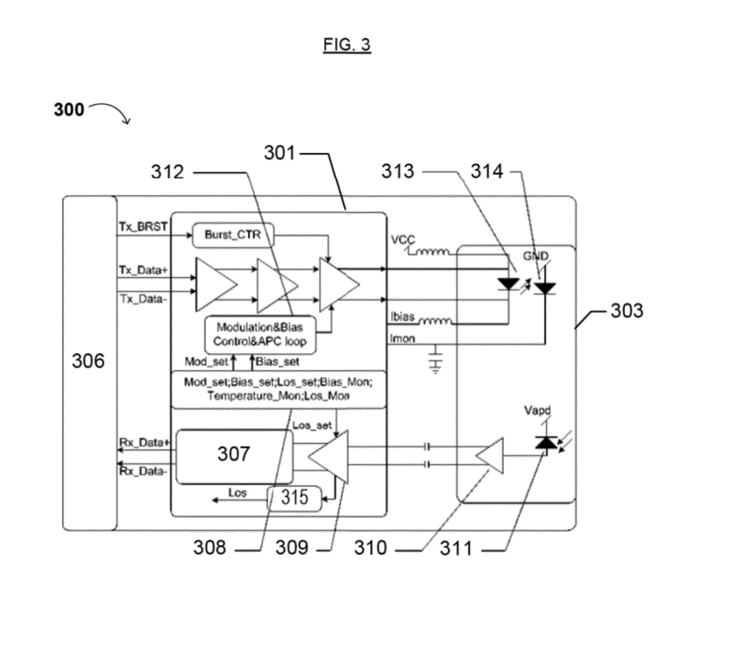
[0013]With respect to conventional technology, the present invention provides a burst laser driver and an RX limiting amplifier capable of operating in a 10 Gb / s network, integrated on a single chip to reduce the cost of the components and the layout space / area of the design. Secondly, the burst laser driver controls the burst signal output of the laser via the control logic and provides an automatic power control loop that allows for current sampling. Deterioration of the optical power due to laser aging is reduced, and burst laser performance can be regulated and adjusted without additional external circuitry (e.g., switching logic and analog sampling circuitry). To realize system performance reporting, the burst optical power indicating circuit and the control logic monitor the burst power, so as to realize system performance reporting. The present limiting amplifier with RX signal indication circuitry and optional clock recovery circuitry satisfies the requirements of 10 Gb / s optical networks with respect to the signal amplitude and fluctuation, ensuring accurate transmission of the optical signals and accurate monitoring of the RX optical signals.
[0014]In various embodiments of the present invention, Optical Line Termination (OLT) bandwidth is allocated by time division multiplexing (TDM; e.g., burst TDM) in an uplink PON system, in which the TX (or circuits thereof) can be turned off by the TX burst energy-saving circuit. When the TX function (e.g., the uplink transmission) is idle, the TX burst holding circuit (e.g., in response to a respective control signal provided by the PON system) turns off the transmitter or a number of circuits in the transmitter, saving energy in and the operational status of the transmitter. When uplink transmissions and / or communications are needed, the transmitting function of the ONU transceiver can be quickly resumed according to the saved operational status.
[0015]Optionally, the ONU transceiver may receive OLT downlink service (e.g., data, instructions, etc.). When downstream operations and data are not received by the system, the RX (and / or circuits thereof) can be turned off according to the respective control signal from the PON system, saving energy in and the operational status of the receiver. When downlink operations are needed, the receiving function of the ONU transceiver can be quickly resumed according to the saved operational status.
[0017]Compared to conventional 10 G ONU technology, the present invention advantageously provides one or more energy-saving control circuits that reduce maximal consumption during transceiver silence, and are capable of switching parts of the transceiver to working or energy-saving modes (e.g., according to external system control logic), ensuring normal communications. The internal control logic (e.g., a microcontroller) can efficiently coordinate all transmitter and receiver functional circuits and allow operational status inquiries. Thus, the present invention overcomes the disadvantage of high power consumption in existing 10 G symmetrical ONU technology, and provides an energy saving circuit for bi-directional transceivers to effectively reduce energy consumption of ONUs in a PON system (e.g., a 10 Gb / s EPON system).

Problems solved by technology

As demand for bandwidth increases, existing 1 G EPON technology is not ideally suited to meet today's needs.
Furthermore, the circuits and optics of conventional 10 G technology consume excessive power, which can affect normal communication.
Thus, it can be difficult to quickly and accurately indicate the output optical power and value.
Additionally, since the optical signal (e.g., the laser) operates at a rate of 10 Gb / s, it can still be problematic to ensure the receiver (RX) receptivity and the ability to monitor the RX optical power in real time.
Furthermore, with existing 10 G solutions, it is difficult to reduce instantaneous power consumption in the 10 G circuit and optics.
Consequently, the PON system 100 may not be able to effectively control the RX energy-saving circuit.

Method used


Image

  • High Speed Bi-Directional Transceiver, Circuits and Devices Therefor, and Method(s) of Using the Same
  • High Speed Bi-Directional Transceiver, Circuits and Devices Therefor, and Method(s) of Using the Same
  • High Speed Bi-Directional Transceiver, Circuits and Devices Therefor, and Method(s) of Using the Same

Examples


Embodiment Construction

[0028]Reference will now be made in detail to various embodiments of the invention, examples of which are illustrated in the accompanying drawing(s). In order to achieve the objectives, technical solutions and advantages of the present invention more clearly, further details of the invention are described below with regard to the Figure(s). While the invention will be described in conjunction with the following embodiments, it will be understood that the descriptions are not intended to limit the invention to these embodiments. On the contrary, the invention is intended to cover alternatives, modifications and equivalents that may be included within the spirit and scope of the invention as defined by the appended claims. Furthermore, in the following detailed description, numerous specific details are set forth in order to provide a thorough understanding of the present invention. However, it will be readily apparent to one skilled in the art that the present invention may be practi...


PUM


Abstract

The present disclosure relates to a high-speed and / or power-saving bi-directional transceiver. The transceiver generally includes a (burst) laser driver; an output power monitoring and indicating circuit; control logic (e.g., a microcontroller unit); bi-directional optics; a photodiode bias control circuit; a limiting amplifier; and a receiver optical power monitoring circuit. Optionally, the present transceiver includes a small form factor pluggable (SFP+) connector housing. In addition, the power-saving bi-directional transceiver generally includes a transmitter (TX) energy-saving circuit, a TX burst holding circuit, a receiver (RX) energy-saving circuit, a RX continuous holding circuit and the control logic.

Description

CROSS REFERENCE TO RELATED APPLICATION[0001]This application claims the benefit of Chinese Patent Application Nos. 201010254908.7 and 201010290187.5, filed on Aug. 17, 2010 and Sep. 25, 2010, respectively, and each of which is incorporated herein by reference as if fully set forth herein.FIELD OF THE INVENTION[0002]The present invention generally relates to the field of optical data communications and network technology. More specifically, embodiments of the present invention pertain to a high speed, bi-directional optical network transceiver, particularly circuits, devices and an optical network unit (ONU) therefor, and method(s) of making and / or using the same. In one embodiment, the transceiver is a small form factor pluggable (e.g., SFP+ compatible) 10 G Ethernet passive optical network (EPON) transceiver. Embodiments of the present invention also pertain to a 10 G bi-direction transceiver with an energy-saving function, circuits and devices therefor, and method(s) of making and...

Claims


Application Information

Patent Timeline
Patent Type & Authority Applications(United States)
IPC IPC(8): H04B10/08H04B10/02
CPCH04B10/40
Inventor JIANG, XUYANG, YILU, YONGSONG, YUAN
Owner SOURCE PHOTONICS
Why Eureka
Try Eureka