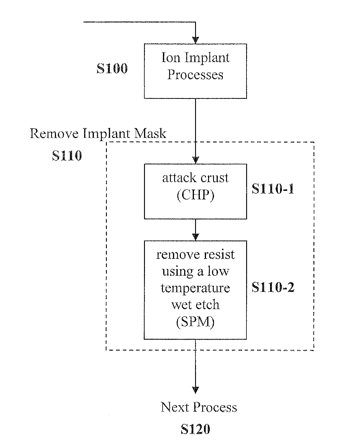
Enhanced stripping of implanted resists
a technology of implanted resists and stripping layers, which is applied in the field of enhanced stripping of implanted resists, can solve the problems of low ph, stripping poses serious safety concerns, and the loss of silicon, so as to reduce the number of process steps, reduce the temperature of wet chemical strips, and reduce the energy footprint of strips
- Summary
- Abstract
- Description
- Claims
- Application Information
AI Technical Summary
Benefits of technology
Problems solved by technology
Method used
Image

Examples
example 1
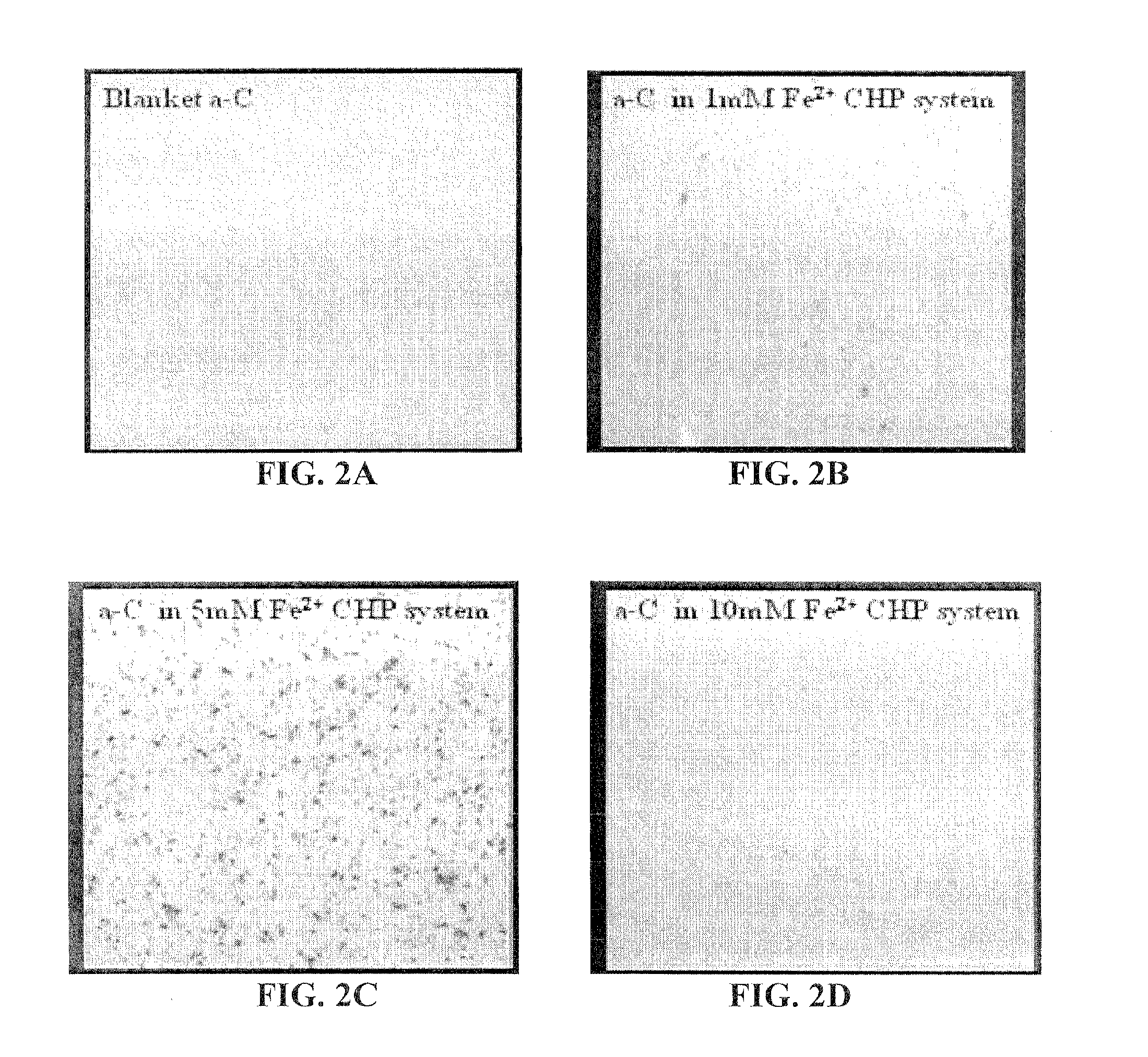
Effectiveness in Attacking Amorphous Carbon Films
[0041]Attack of amorphous carbon films was investigated by immersing the carbon films in CHP solution for 30 minutes at room temperature followed by rinsing in DI water. It is believed that the carbonized crust on photoresist is amorphous carbon. Accordingly, amorphous carbon was used in the initial experiments. The films were then immersed in HCl (1 M) for 2 minutes to remove residual iron. CHP solutions (pH˜2.8) containing 20% H2O2 and different Fe2+ levels (1 mM, 5 mM, 10 mM) were used to compare the effects of Fe2+ levels on the ability to attack the carbon film. FIGS. 2A-2D illustrate the results of this test. Specifically, FIGS. 2A-2D show optical microscopic images (magnification 1000×) of amorphous carbon films after CHP treatment where FIG. 2A shows a blanket carbon film before processing, FIG. 2B shows the blanket carbon film after treatment in 1 mM Fe2+ CHP chemical system, FIG. 2C shows the blanket carbon film after treatm...
example 2
Effectiveness of Photoresist Removal
[0044]Field Emission SEM was used to characterize the response of implanted resist films to treatment in 2:1 SPM before and after treatment in CHP. FIGS. 3A-3C show cross-sectional FESEM images of (1016 As / cm2) implanted PR after different treatments. Specifically, FIG. 3A shows a blanket photoresist film on a silicon substrate, FIG. 3B shows the substrate after a photoresist film is immersed only in (2:1) SPM, and FIG. 3C shows the substrate after a photoresist film is pretreated with CLIP followed by immersion in 2:1 SPM. Referring to FIG. 3A, blanket PR showed crust layer of thickness ˜400 nm. Upon treatment in 2:1 SPM for 5 minutes, the resist film shows poor removal, as seen in FIG. 3B. However, as shown in FIG. 3C, excellent removal of high dose implanted PR is possible by first exposing the resist to CHP solution containing 5 mM Fe2+ and 20% H2O2 for 15 minutes followed by 5 minutes immersion in 2:1 Sulfuric acid-Peroxide Mixture (SPM) at 8...
example 3
Crust Disruption Using UV / H2O2 CHP Chemical System
[0049]High dose implant resist stripping using the UV / H2O2 CHP chemical system was explored. A blanket PR exposed to arsenic ion dose of 1016 / cm2 was exposed to UV (254 nm) radiation for a predetermined period of time and then subjected to a H2O2 solution under UV irradiation for a second predetermined period of time. For the example embodiment, the concentration of H2O2 in the solution was 20% and the PR was treated with the solution under UV radiation for 15 minutes. The PR was then treated to a 2:1 SPM with sulfuric acid preheated to a temperature of 80° C. and mixed with hydrogen peroxide that was at about 10° C.
[0050]FIGS. 8A and 8B show 3D confocal images of a line scan on the removal region of a substrate after 5 minutes of UV exposure and UV / H2O2 treatment (FIG. 8A) and 10 minutes UV of exposure and UV / H2O2 treatment (FIG. 8B) in accordance with embodiments of the invention.
[0051]As illustrated by the figures, the higher the ...
PUM
 Abstract
Description
Claims
Application Information
 - Generate Ideas
- Intellectual Property
- Life Sciences
- Materials
- Tech Scout
- Unparalleled Data Quality
- Higher Quality Content
- 60% Fewer Hallucinations
Browse by: Latest US Patents, China's latest patents, Technical Efficacy Thesaurus, Application Domain, Technology Topic, Popular Technical Reports.
© 2025 PatSnap. All rights reserved.Legal|Privacy policy|Modern Slavery Act Transparency Statement|Sitemap|About US| Contact US: help@patsnap.com