Singulated semiconductor device separable electrical interconnect

a semiconductor device and separable technology, applied in the field of socket assembly, can solve the problems of difficult repair, inability of the ic device to connect to the final pcb, and small size and distance between the die terminals, and achieve the effects of improving the test performance of the system, large surface area, and high performance test capability

Active Publication Date: 2012-03-08
HSIO TECH
View PDF5 Cites 64 Cited by
  • Summary
  • Abstract
  • Description
  • Claims
  • Application Information

AI Technical Summary

Benefits of technology

[0013]There are few or no commercial products available today to allow a semiconductor manufacturer to validate the IC device directly off of the singulated die, with process or performance information provided in a manner much faster than if the die is tested after packaging. In most cases today, in order to provide any high performance test capability, the user must probe the die in an expensive wafer probe system with expensive probes. In many cases, full functionally testing of the IC device on the wafer is not possible. The present socket assembly allows the user to power and manage the IC device to be tested. This test capability allows the IC device manufacturer to segregate the performance of the IC devices before packaging vs. after packaging.
[0014]The ability to build multi-layer structures compliant printed circuit with a relatively large surface area is a major advantage, and the ability to add electrical enhancements provides performance advantages over existing probe products. For example, the ability to add programmable logic, transistors, and memory device to the present socket assembly provides an opportunity to incorporate test intelligence into the assembly, extending the use of legacy test equipment or improving the test performance of the system.
[0015]Transistors and memory printed into the socket assembly provide adaptive testing or the ability to alter the circuit being tested. The present socket assembly also permits interconnecting a group of IC devices to simulate a multi-chip or system-in-package configuration, so that the IC devices can be tested in relation to the other chips they will eventually be expected to interact with.
[0016]The present socket assembly provides a low cost alternative to other socket products, by utilizing an additive printing process and unique contact member fabrication process. The nature of the process can allow for very high frequency performance, as well as the addition of on-board electrical devices and circuitry planes that are not available with other socket products. The present socket assembly can be superior to membrane socket products in terms of mechanical performance, manufacturing complexity, electrical performance, and cost.
[0017]The present disclosure is also directed to a method of making a socket assembly that forms a solderless electrical connection between terminals on a singulated integrated circuit device and another circuit member. A base layer of a dielectric material is printed onto a surface of a fixture, while leaving cavities in the fixture exposed. A conductive material is printed into a plurality of the cavities in the fixture. At least one dielectric layer is printed with recesses corresponding to a target circuit geometry on the dielectric base layer. A conductive material is deposited in at least a portion of the recesses comprising conductive traces electrically coupled to the contact members of a compliant printed circuit. The compliant printed circuit is removed from the fixture to expose distal ends of the contact members. The compliant printed circuit is positioned relative to an opening in a socket housing so the contact members electrically couple with the terminals on a singulated integrated circuit device located in the opening. Compliant layers can optionally be printed on the compliant printed circuit to increase performance of the present socket assemblies.
[0018]The present disclosure is also directed to a method of adaptive testing of singulated semiconductor devices using the socket assembly of the present disclosure. Electrical devices on the socket assembly can monitor performance of the circuit member being tested and signal the test station to modify the test protocol accordingly. The test station can also be signaled to modify the circuit member.

Problems solved by technology

In many cases, the size and distance between die terminals is so small that the IC device cannot be connected to the final PCB without some sort of re-routing interface.
Regardless of whether a package is under filled with epoxy, the connection of the IC device to the package is generally not reworkable after packaging, and if there is a missing or broken connection it is difficult to repair.
If the packaged IC device fails testing then the cost of the package and manufacturing process is lost.
In general, the area array packaging is more expensive due to the larger pin counts and more sophisticated substrates required.
The limitations for area array packaging include the terminal pitch, thermal management, cost, ability to rework faulty IC devices and reliability of the solder joints.
There also have been advancements in recent years in both area array packaging and peripheral lead packaging where multiple IC devices are placed in the same package, creating what has been nicknamed SiP for “system in package.” Placing multiple IC devices in a single package further complicates the problems discussed above.

Method used


Image

  • Singulated semiconductor device separable electrical interconnect
  • Singulated semiconductor device separable electrical interconnect
  • Singulated semiconductor device separable electrical interconnect

Examples


Embodiment Construction

[0035]The present disclosure relates to a high performance socket assembly capable of interconnecting one or more IC devices in a solderless interface, permitting the IC device to be tested prior to final packaging. The present socket assembly can be used with IC devices having contact-to-contact spacing (pitch) on the order of less than about 1.0 millimeter (1×10⁻³ meters), and more preferably a pitch of less than about 0.7 millimeter, and most preferably a pitch of less than about 0.4 millimeter.

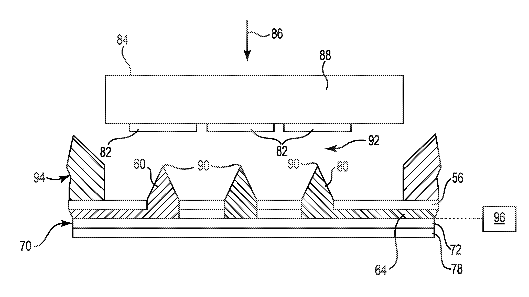
[0036]FIG. 1 is a cross-sectional view of a fixture 50 useful in making a compliant printed circuit for a socket assembly in accordance with an embodiment of the present disclosure. The fixture 50 can include a plurality of cavities 52 in a first surface 54. The locations of the cavities 52 are arranged in an array that corresponds to terminals on a wafer-level IC device (see e.g., FIG. 6). The cavities 52 can be formed using a variety of techniques, such as molding, machining, printing, i...


PUM

PropertyMeasurementUnit
aspect ratioaaaaaaaaaa
widthaaaaaaaaaa
conductiveaaaaaaaaaa

Abstract

A socket assembly that forms a solderless electrical interconnection between terminals on a singulated integrated circuit device and another circuit member. The socket housing has an opening adapted to receive the singulated integrated circuit device. The compliant printed circuit is positioned relative to the socket housing to electrically couple with the terminals on a singulated integrated circuit device located in the opening. The compliant printed circuit includes a dielectric base layer printed onto a surface of a fixture, while leaving cavities in the surface of the fixture exposed. A plurality of contact members are formed in the plurality of cavities in the fixture and coupled to the dielectric base layer. The contact members are exposed wherein the compliant printed circuit is removed from the fixture. At least one dielectric layer with recesses corresponding to a target circuit geometry is printed on the dielectric base layer. A conductive material is deposited in at least a portion of the recesses to form conductive traces electrically coupling the contact members to the other circuit member.

Description

TECHNICAL FIELD[0001]The present disclosure relates to a socket assembly produced using additive printing processes that is capable of interconnecting one or more singulated die devices in a separable or solderless fashion to another circuit member, such as for example a test station. The present socket assembly allows the singulated die devices to be tested prior to final packaging.BACKGROUND OF THE INVENTION[0002]Traditional semiconductors and IC devices are typically formed on a substrate using photolithography. The substrate may be a silicon wafer. Multiple IC devices are typically formed on a single wafer and then the wafer is cut into die. The IC devices are typically packaged in a variety of ways to provide redistribution from the terminals on the die to a spacing that is conducive to cost effective printed circuit board (PCB) fabrication techniques. The package also serves to protect the fragile silicon or provide additional functions such as thermal management or near devic...

Claims


Application Information

Patent Timeline
Patent Type & Authority Applications(United States)
IPC IPC(8): H01R12/71
CPCG01R1/0491G01R3/00G01R1/0735Y10T29/49126Y10T29/49128Y10T29/49155Y10T29/49169Y10T29/49204Y10T29/49222
Inventor RATHBURN, JAMES
Owner HSIO TECH
Why Eureka
Try Eureka