Semiconductor device and light-emitting device, and manufactuirng method thereof

a technology of semiconductor devices and light-emitting devices, which is applied in the direction of organic semiconductor devices, solid-state devices, thermoelectric devices, etc., can solve the problems of affecting the reliability of semiconductor devices, difficult to completely remove moisture from semiconductor devices, and/or to completely prevent moisture entry from the air, etc., to achieve high-reliable semiconductor devices and high-reliable light-emitting devices

Inactive Publication Date: 2012-03-15
SEMICON ENERGY LAB CO LTD
View PDF19 Cites 21 Cited by
  • Summary
  • Abstract
  • Description
  • Claims
  • Application Information

AI Technical Summary

Benefits of technology

[0034]According to the present invention, a highly reliable semiconductor device using an oxide semiconductor

Problems solved by technology

There is a problem in that a transistor that has a channel formation region using an oxide semiconductor, which is of an enhancement (also referred to as normally-off) type, has changed into a depletion (also referred to as normally-on) type due to the use.
A change of a transistor using an oxide semiconductor into a depletion type over time, which is a problem impairing the reliability of the semiconductor device, occurs particularly in a semiconductor device i

Method used


Image

  • Semiconductor device and light-emitting device, and manufactuirng method thereof
  • Semiconductor device and light-emitting device, and manufactuirng method thereof
  • Semiconductor device and light-emitting device, and manufactuirng method thereof

Examples


embodiment 1

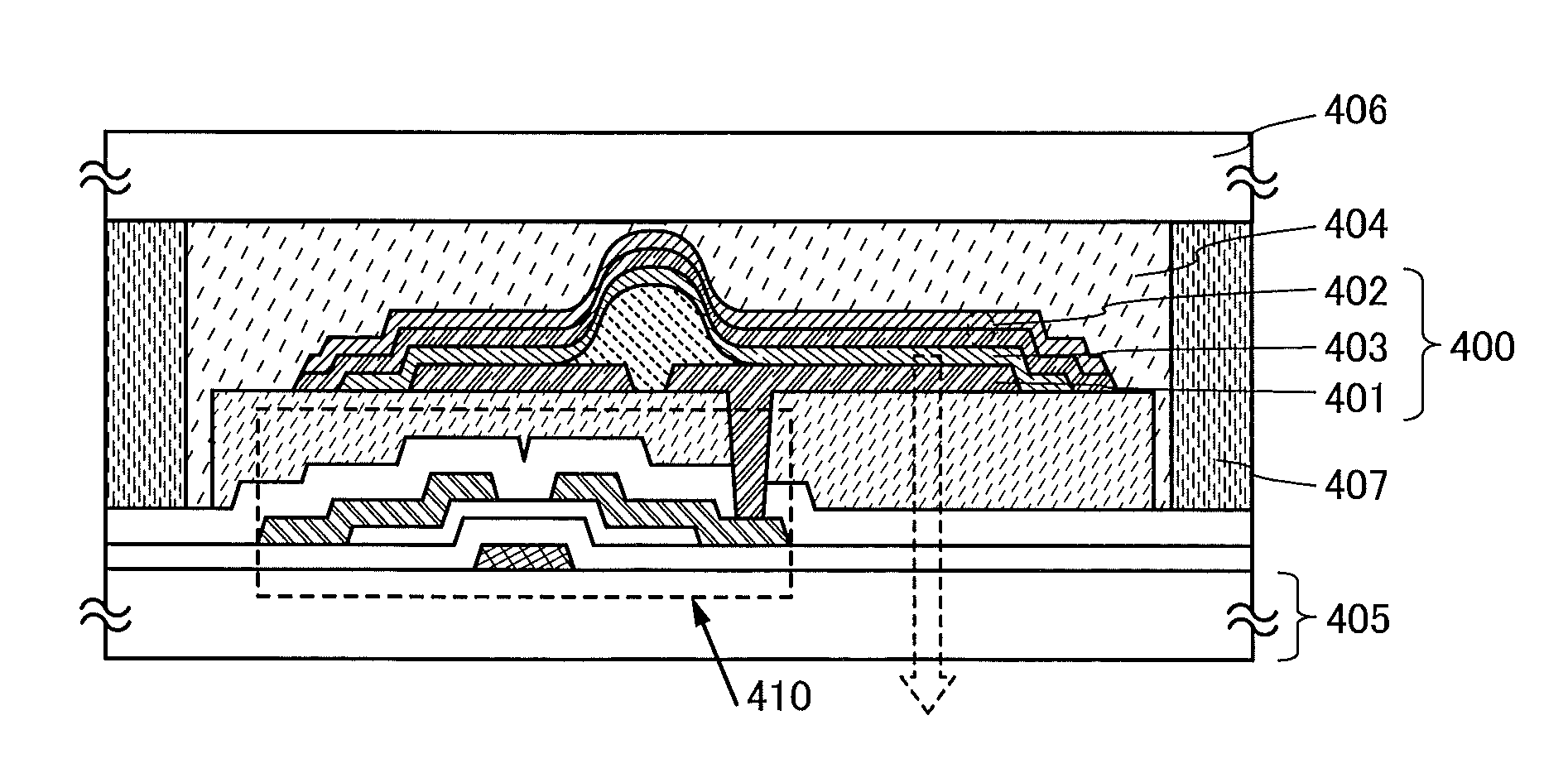
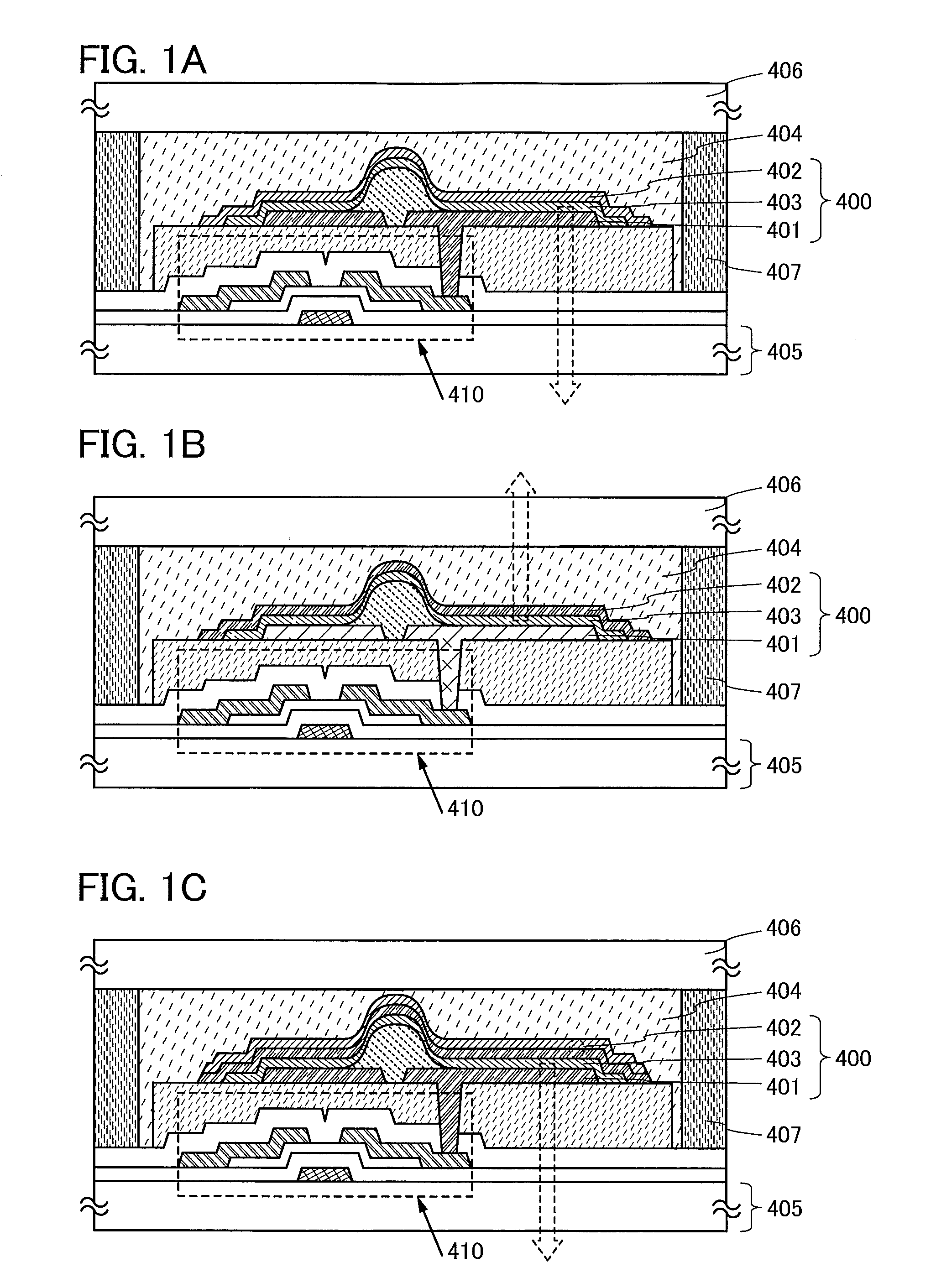
[0045]In this embodiment, a structure of a semiconductor device including a semiconductor element using an oxide semiconductor and a light-emitting element in which an organic layer containing a light-emitting substance is provided between a first electrode and a second electrode will be described with reference to FIGS. 1A to 1C. Note that because an inert, electrically conductive material is used for the second electrode of the light-emitting element given as an example in this embodiment, the reduction of an impurity including a hydrogen atom (e.g., moisture) and production of a hydrogen ion or a hydrogen molecule hardly occur.

[0046]The semiconductor device described in this embodiment is a light-emitting device having a transistor and the light-emitting element connected to the transistor. The light-emitting element can also be used for a pixel portion of the light-emitting display device by being provided in matrix arrangement.

[0047]In the semiconductor device given as an examp...

embodiment 2

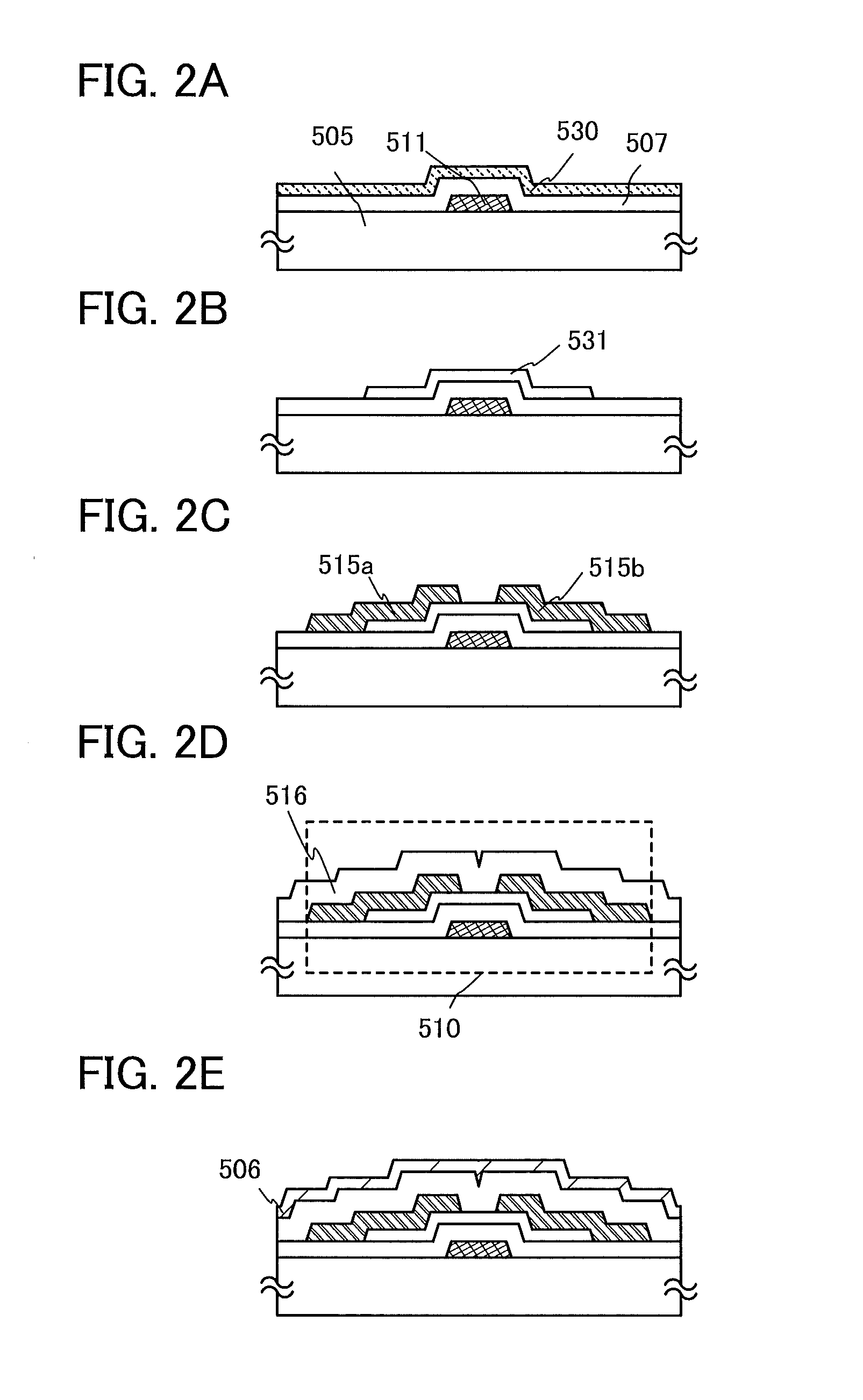
[0060]In this embodiment, a transistor that has a channel formation region using an oxide semiconductor will be described. The enhancement-type transistor that has a channel formation region using an oxide semiconductor has a gate electrode on one side of a gate insulating film, an oxide semiconductor layer on the other side of the gate insulating film, and a source and drain electrode layers which are in contact with the oxide semiconductor layer and whose end portions are overlapped with the gate electrode. In this embodiment, as an example of the enhancement-type transistor that has a channel formation region using an oxide semiconductor, a structure of an inverted staggered transistor using an oxide semiconductor and a manufacturing method thereof will be described with reference to FIGS. 2A to 2E. Note that the transistor is not limited to an inverted staggered transistor, and the transistor may be a staggered transistor, a coplanar transistor, or an inverted coplanar transisto...

embodiment 3

[0146]In this embodiment, a structure of a light-emitting element applicable to the semiconductor device described in Embodiment 1 and a method for manufacturing the light-emitting element will be described with reference to FIG. 4. Specifically is described a light-emitting element including a first electrode that is electrically connected to a source and drain electrode layers of a transistor that has a channel formation region using an oxide semiconductor and is one of an anode and a cathode, a second electrode that is the other thereof, and an organic layer containing a light-emitting substance between the first electrode and the second electrode.

[0147]FIG. 4 illustrates one example of a structure of a light-emitting element which can be used for a light-emitting device given as an example in this embodiment. In the light-emitting element illustrated in FIG. 4, one of the first and second electrodes is an anode 1101 and the other thereof is a cathode 1102, between which an organ...


PUM


Abstract

In a semiconductor device including an organic layer containing a light-emitting substance between a first electrode connected to a source or drain electrode layer of an enhancement-type transistor that has a channel formation region using an oxide semiconductor and a second electrode overlapped with the first electrode, an active, electrically conductive material which produces a hydrogen ion or a hydrogen molecule by reducing an impurity including a hydrogen atom (e.g., moisture) is excluded from the second electrode. The semiconductor device including an oxide semiconductor is formed using especially an inert, electrically conductive material which hardly causes production a hydrogen ion or a hydrogen molecule by reacting with water. Specifically, the semiconductor device is formed using any of a metal, an alloy of metals, and a metal oxide each having a higher oxidation-reduction potential than the standard hydrogen electrode.

Description

BACKGROUND OF THE INVENTION[0001]1. Field of the Invention[0002]The present invention relates to a semiconductor device and a light-emitting device each using an oxide semiconductor and a manufacturing method thereof.[0003]Note that the semiconductor device in this specification refers to all devices including a semiconductor element that can function by utilizing semiconductor characteristics; semiconductor circuits, light-emitting devices, display devices, and electronic devices are all semiconductor devices.[0004]2. Description of the Related Art[0005]A technique in which a transistor is formed using a semiconductor material such as amorphous silicon, polysilicon, or transferred single crystal silicon over a substrate having an insulating surface has been known. While a transistor including amorphous silicon has low field effect mobility, the transistor can be easily formed over a large-area glass substrate. On the other hand, while a transistor including polycrystalline silicon ...

Claims


Application Information

Patent Timeline
IPC IPC(8): H01L27/32
CPCH01L27/1225H01L27/3262H01L27/3272H01L29/7869H01L51/5068H01L2251/5323H01L51/5231H01L51/5234H01L51/524H01L51/5278H01L2251/554H01L51/5092H10K59/126H10K59/1213H10K50/157H10K50/171H10K50/19H10K2102/3031H10K2101/50H10K59/80524H10K59/871H10K59/80523H10K50/828H10K50/826H10K50/841
Inventor SUGISAWA, NOZOMUHATANO, KAORUSEO, SATOSHI
Owner SEMICON ENERGY LAB CO LTD
Why Eureka
Try Eureka