Compliant printed circuit area array semiconductor device package

a semiconductor device and printed circuit technology, applied in semiconductor devices, semiconductor/solid-state device details, electrical apparatus, etc., can solve the problems of difficult repair, inability to connect ic devices to final pcbs, and small size and distance between die terminals, and achieve excellent electrical performance and low cos

Active Publication Date: 2012-03-15
KONINKLIJKE PHILIPS ELECTRONICS NV +1
View PDF15 Cites 73 Cited by
  • Summary
  • Abstract
  • Description
  • Claims
  • Application Information

AI Technical Summary

Benefits of technology

[0008]The present application relates to a compliant array IC device package (IC package). The present IC

Problems solved by technology

In many cases, the size and distance between die terminals is so small that the IC device cannot be connected to the final PCB without some sort of re-routing interface.
Regardless of whether a package is under filled with epoxy, the connection of the IC device to the package is generally not reworkable after packaging, and if there is a missing or broken connection it is difficult to repair.
If the packaged IC device fails testing then the cost of the package and manufacturing process is lost.
In general, the area array packaging is more expensive due to

Method used


Image

  • Compliant printed circuit area array semiconductor device package
  • Compliant printed circuit area array semiconductor device package
  • Compliant printed circuit area array semiconductor device package

Examples


Embodiment Construction

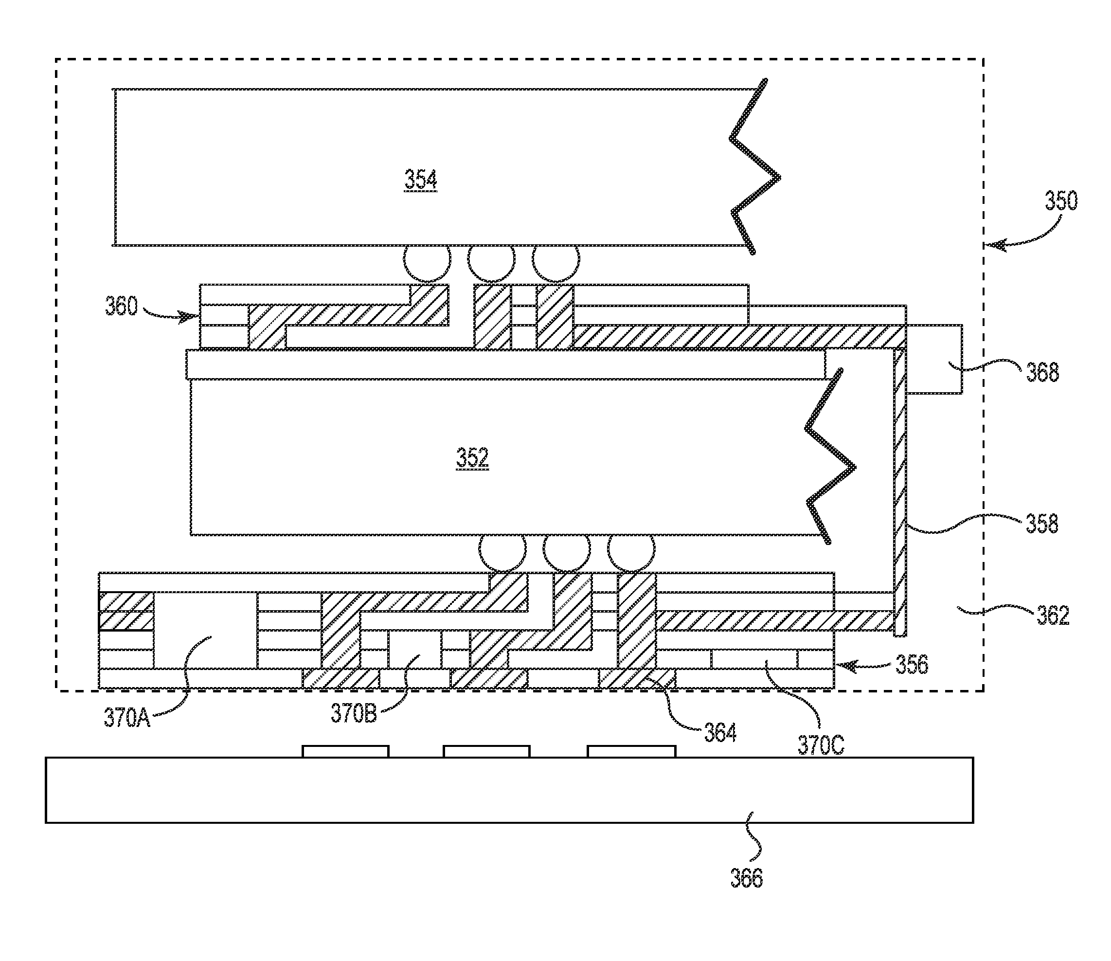
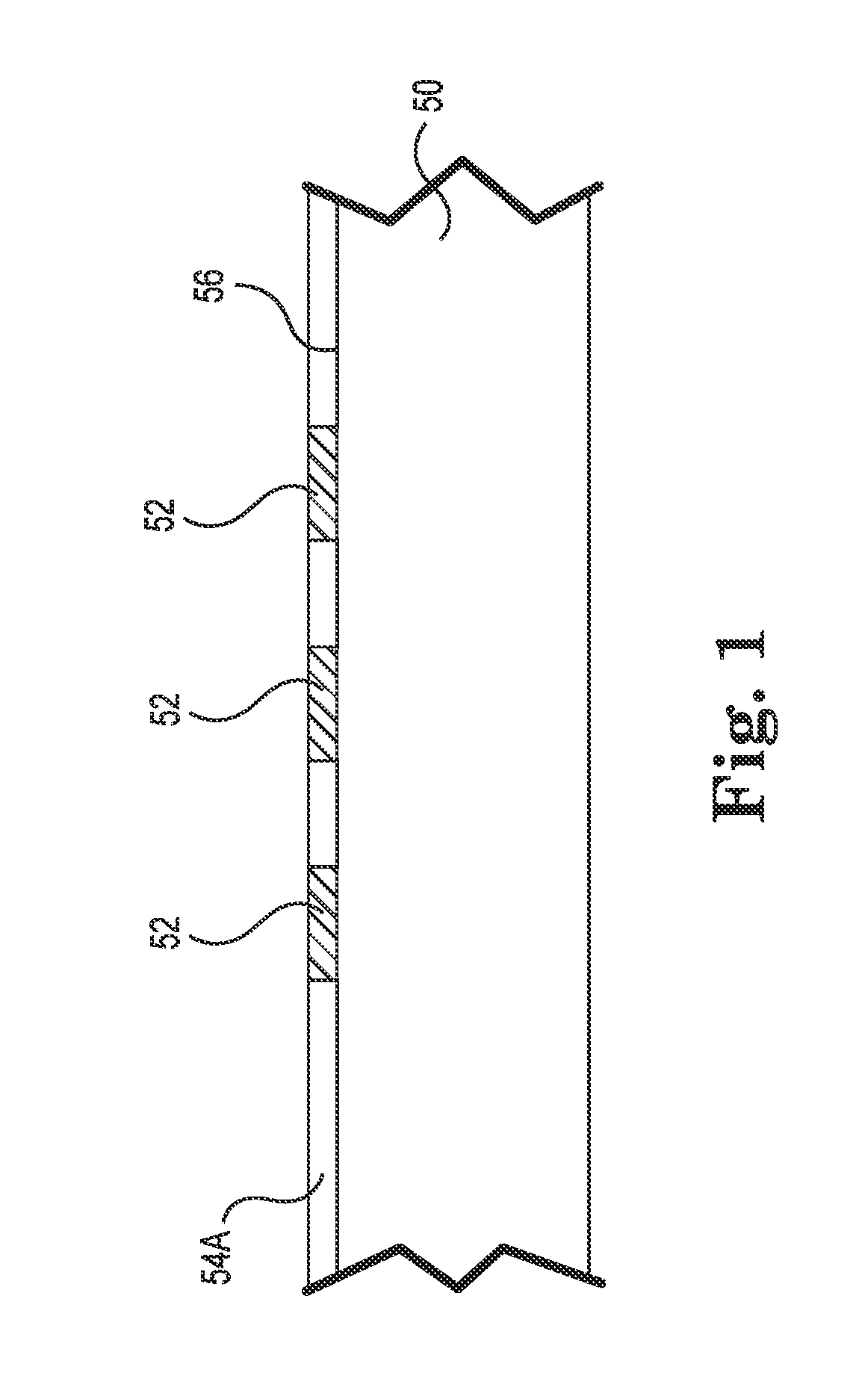
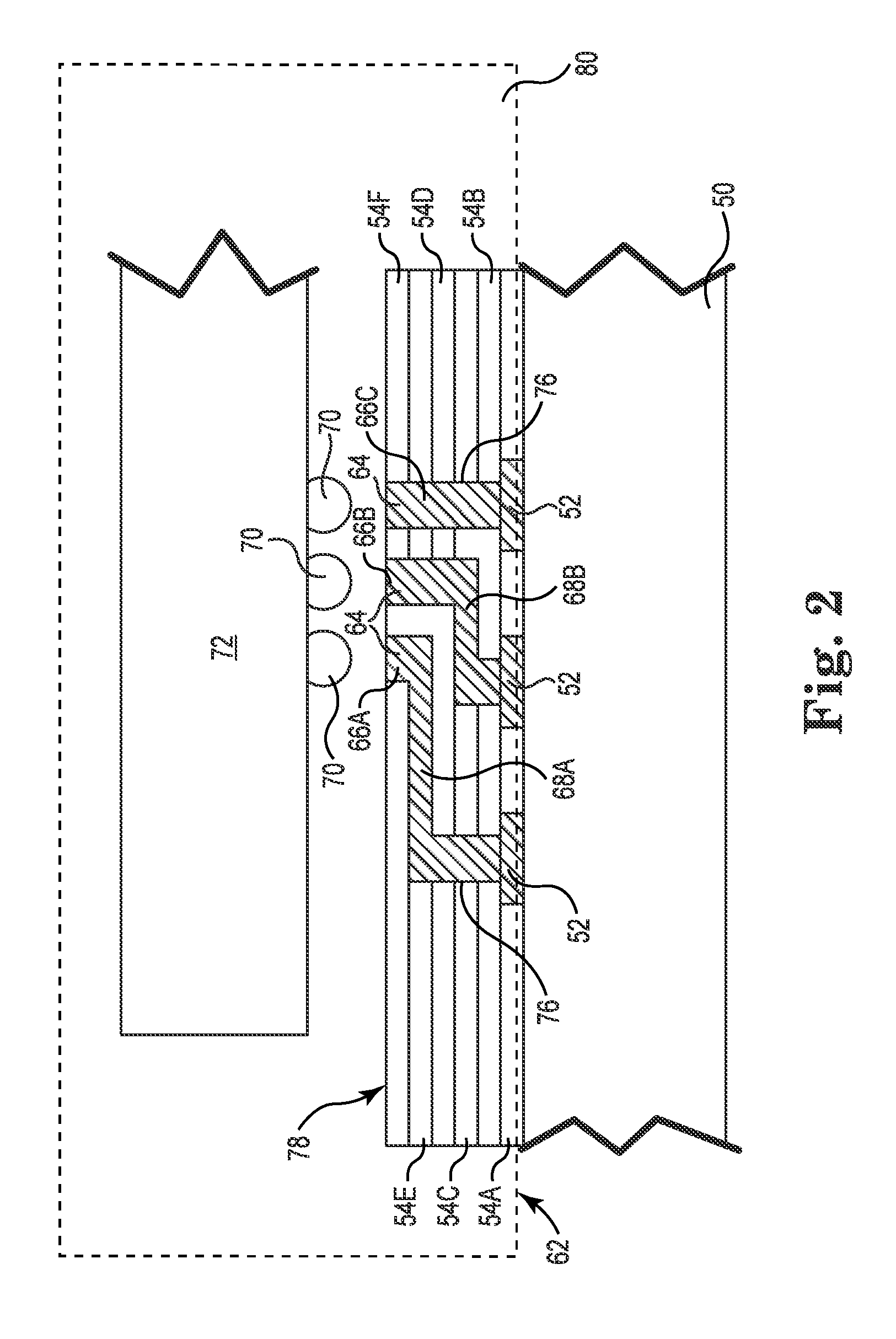
[0039]The present disclosure is directed to a compliant array IC package that is inexpensive to produce, has relative long life and provides excellent electrical performance. An IC package according to the present disclosure can be formed by an additive printing process to provide a high performance IC package capable of interconnecting a single device or multiple IC devices, while providing at or near terminal compliance to increase interconnect reliability. The unique nature of the additive printing process can allow direct writing of circuitry and dielectrics, while also allowing stress decoupling at the terminal joints as well as embedded function not seen in traditional IC packaging.

[0040]Printable silicon inks provide the ability to print electrical devices. Exemplary embodiments of printable silicone inks are disclosed, for example, in U.S. Pat. No. 7,485,345 (Renn et al.); U.S. Pat. No. 7,382,363 (Albert et al.); U.S. Pat. No. 7,148,128 (Jacobson); U.S. Pat. No. 6,967,640 (A...


PUM


Abstract

An integrated circuit (IC) package for an IC device, and a method of making the same. The IC package includes an interconnect assembly with at least one printed compliant layer, a plurality of first contact members located along a first major surface, a plurality of second contact members located along a second major surface, and a plurality of printed conductive traces electrically coupling a plurality of the first and second contact members. The compliant layer is positioned to bias at least the first contact members against terminals on the IC device. Packaging substantially surrounds the IC device and the interconnect assembly. The second contact members are accessible from outside the packaging.

Description

TECHNICAL FIELD[0001]The present disclosure relates to a compliant array integrated circuit (IC) device package, and in particular, to a compliant IC device package made using an additive printing process.BACKGROUND OF THE INVENTION[0002]Traditional semiconductors and IC devices are typically formed on a substrate using photolithography. The substrate may be a silicon wafer. Multiple IC devices are typically formed on a single wafer and then the wafer is cut into die. The IC devices are typically packaged in a variety of ways to provide redistribution from the terminals on the die to a spacing that is conducive to cost effective printed circuit board (PCB) fabrication techniques. The package also serves to protect the fragile silicon or provide additional functions such as thermal management or near device decoupling. In many cases, the size and distance between die terminals is so small that the IC device cannot be connected to the final PCB without some sort of re-routing interfac...

Claims


Application Information

Patent Timeline
IPC IPC(8): H01L23/48H01L21/50H01L21/20
CPCH01L21/4867H01L2224/16235H01L23/4985H01L23/552H01L23/66H01L24/16H01L24/90H01L2221/68345H01L2223/6677H01L2924/01013H01L2924/01029H01L2924/01049H01L2924/01078H01L2924/01079H01L2924/01082H01L2924/09701H01L2924/12044H01L2924/14H01L2924/15174H01L2924/19041H01L2924/19042H01L2924/19043H01L2924/3011H01L2924/3025H01L2924/01006H01L2924/01033H01L2924/01047H01L2924/01075H01L2924/014H01L2225/06527H01L2225/06517H01L2225/06572H01L2224/81191H01L2924/1306H01L23/49822H01L2924/00H01L2924/15787H01L2224/0557H01L2224/05573H01L2924/00014H01L2224/05571H01L2224/0554H01L2224/05599H01L2224/0555H01L2224/0556
Inventor RATHBURN, JAMES
Owner KONINKLIJKE PHILIPS ELECTRONICS NV
Why Eureka
Try Eureka