Semiconductor substrate, semiconductor device and method of manufacturing a semiconductor substrate

a semiconductor substrate and semiconductor technology, applied in the field of semiconductor substrates, can solve the problems of limited dislocation-free areas in this case, essentially non-equilibrium defects of tds, and narrow devices such as laser diodes, and achieve the effect of reducing the density of threading dislocation

Inactive Publication Date: 2012-03-15
ODNOBLYUDOV MAXIM +3
View PDF2 Cites 3 Cited by
  • Summary
  • Abstract
  • Description
  • Claims
  • Application Information

AI Technical Summary

Benefits of technology

[0016]A semiconductor device in accordance with the present invention is characterized by what is presented in claim 4. The semiconductor device is made of nitrides of group III metals having wurtzite crystal structure and grown in vapor phase either on a (0001) oriented foreign substrate, lattice mismatched to the semiconductor device materials, or on existing (0001) oriented highly dislocated layer of the semiconductor device materials. The device comprises a semiconductor substrate and device layers positioned above said substrate. According to the present invention, the semiconductor substrate comprises a dislocation redirection layer, in which inclination of threading dislocations towards high index crystallographic planes, having indexes other than (0001) and those of the type {1 100}, is arranged in order to enhance the probability of the threading dislocations to meet each other; and a dislocation reaction layer, in which the threading dislocations coalesce with each other resulting in reduced threading dislocation density at the semiconductor substrate surface. The semiconductor device can be e.g. a LED or a laser diode. Clear advantages are achieved with this structure in form of better quality of the device layers due to the low dislocation density throughout the semiconductor substrate surface.
[0030]The present invention provides essential advantages compared to the prior art. The substrate according to the invention can have drastically reduced threading dislocation density throughout the surface and is thus well suitable for further epitaxial growth of device layers. The manufacturing method of the invention includes only in situ process steps while many variations of traditional methods necessitate unwanted ex situ processing. The method of the invention is also well controllable in contrast to e.g. micromasking method of the prior art including random mask coverage.

Problems solved by technology

Despite of their high density, TDs are essentially non-equilibrium defects.
However dislocation-free areas in this case are limited to the narrow stripes above dielectric stripes.
Therefore these techniques can only be used for narrow devices like laser diodes.
One of the disadvantages of these variations is that they are ex situ processes.
The efficiency of these techniques is limited by the fact that the mask regions are distributed randomly and do not provide selective treatment of the dislocated regions.
According to the preceding prior art description, despite of all development in the area the known solutions still have plenty of drawbacks and weaknesses.

Method used


Image

  • Semiconductor substrate, semiconductor device and method of manufacturing a semiconductor substrate
  • Semiconductor substrate, semiconductor device and method of manufacturing a semiconductor substrate
  • Semiconductor substrate, semiconductor device and method of manufacturing a semiconductor substrate

Examples


Embodiment Construction

[0041]Reference will now be made in detail to the embodiments and examples relating to the present invention, which are illustrated in the accompanying figures.

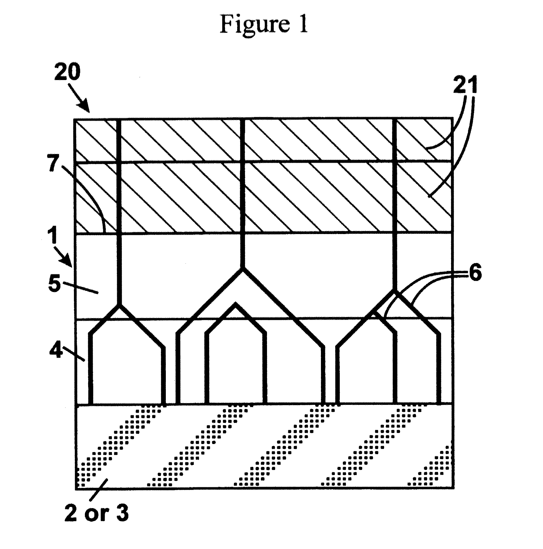
[0042]The semiconductor device 20 of FIG. 1 comprises a semiconductor substrate 1. Semiconductor substrate includes a foreign substrate 2 or a highly dislocated layer 3 of the semiconductor substrate materials, a dislocation redirection layer 4 and a dislocation reaction layer 5. Device layers 21 are grown on the semiconductor substrate surface 7. Threading dislocations (TDs) 6 formed in the early stage of the dislocation redirection layer 4 growth deviate upper in the layer from the initially vertical orientation. In the dislocation reaction layer 5 TDs 6 coalesce with each other thus reducing the dislocation density of the semiconductor substrate 1. As result, the semiconductor substrate surface 7 is of high crystalline quality with a low dislocation density and as such well suitable for further growing of the device layers...


PUM

PropertyMeasurementUnit
temperatureaaaaaaaaaa
total thicknessaaaaaaaaaa

Abstract

A semiconductor substrate of the present invention is made of nitrides of group III metals having wurtzite crystal structure and is grown in vapor phase either on a (0001) oriented foreign substrate (2), lattice mismatched to the semiconductor substrate materials, or on existing (0001) oriented highly dislocated layer (3) of the semiconductor substrate materials and has a highly reduced dislocation density. According to the present invention, a structure is utilized for the dislocation density reduction, which comprises a dislocation redirection layer (4) providing intentional inclination of threading dislocations (6) towards high index crystallographic planes having crystallographic indexes other than (0001) and those of the type {1 100}, in order to enhance the probability for dislocation reactions; and a dislocation reaction layer (5) positioned above said dislocation layer (4), in which the threading dislocations (6) coalesce with each other resulting in reduced threading dislocation density at the semiconductor substrate surface (7).

Description

[0001]This application is a divisional filing of U.S. application Ser. No. 11 / 792,687, filed May 30, 2008, the disclosure of which is incorporated herein by reference.FIELD OF THE INVENTION[0002]The invention relates in general to a semiconductor substrate with reduced threading dislocation density. More particularly, the semiconductor substrate is formed of nitrides of group III metals with wurtzite crystal structure and grown in vapor phase either on a (0001) oriented foreign substrate, lattice mismatched to the semiconductor substrate materials, or on existing (0001) oriented highly dislocated layer formed of the semiconductor substrate materials. The invention also relates to a device utilizing and a method of manufacturing such substrate.BACKGROUND OF THE INVENTION[0003]Growth of (0001) oriented nitrides of group III metals with wurtzite crystal structure on a foreign substrate with large lattice mismatch, e.g. sapphire, silicon carbide, silicon, or zinc oxide, occurs via forma...

Claims


Application Information

Patent Timeline
Patent Type & Authority Applications(United States)
IPC IPC(8): H01L21/20H01LH01L29/04H01L29/20
CPCH01L29/2003H01L29/045H01L21/02458H01L21/0254H01L21/02505H01L21/0242H01L21/20
Inventor ODNOBLYUDOV, MAXIMBOUGROV, VLADISLAVROMANOV, ALEXEILANG, TEEMU
Owner ODNOBLYUDOV MAXIM
Why Eureka
Try Eureka