Integrated MOSFET Device and Method with Reduced Kelvin Contact Impedance and Breakdown Voltage

a technology of mosfet and kelvin, which is applied in the direction of semiconductor devices, diodes, electrical apparatus, etc., can solve the problems of reducing the breakdown voltage, undesirable increase of the kelvin contact impedance, and the problem of more pronounced problem

Active Publication Date: 2012-03-22
ALPHA & OMEGA SEMICON INC
View PDF4 Cites 15 Cited by
  • Summary
  • Abstract
  • Description
  • Claims
  • Application Information

AI Technical Summary

Benefits of technology

[0021]Similar to device 100, device 102 also includes implants with dopants having the same carrier type as the epitaxial layer. The resulting epi enhancement portions (also referred to as breakdown voltage reducing implants) 182a and 182b are formed below diode enhancement layers 185a and 185b, and have the same carrier type as the epitaxial layer but at a higher concentration to reduce the breakdown voltage of the low injection diodes thus preventing the electric field from causing damage to the gate oxide.

Problems solved by technology

As device size decreases, the correspondingly reduced contact electrode area and thickness of gate oxide within the device typically result in an undesirable increase of its Kelvin contact impedance and reduction of its breakdown voltage.
The problem is more pronounced in power MOSFET devices, which often conduct high current and demand high breakdown voltage.

Method used


Image

  • Integrated MOSFET Device and Method with Reduced Kelvin Contact Impedance and Breakdown Voltage
  • Integrated MOSFET Device and Method with Reduced Kelvin Contact Impedance and Breakdown Voltage
  • Integrated MOSFET Device and Method with Reduced Kelvin Contact Impedance and Breakdown Voltage

Examples


Embodiment Construction

[0012]The description above and below plus the drawings contained herein merely focus on one or more currently preferred embodiments of the present invention and also describe some exemplary optional features and / or alternative embodiments. The description and drawings are presented for the purpose of illustration and, as such, are not limitations of the present invention. Thus, those of ordinary skill in the art would readily recognize variations, modifications, and alternatives. Such variations, modifications and alternatives should be understood to be also within the scope of the present invention.

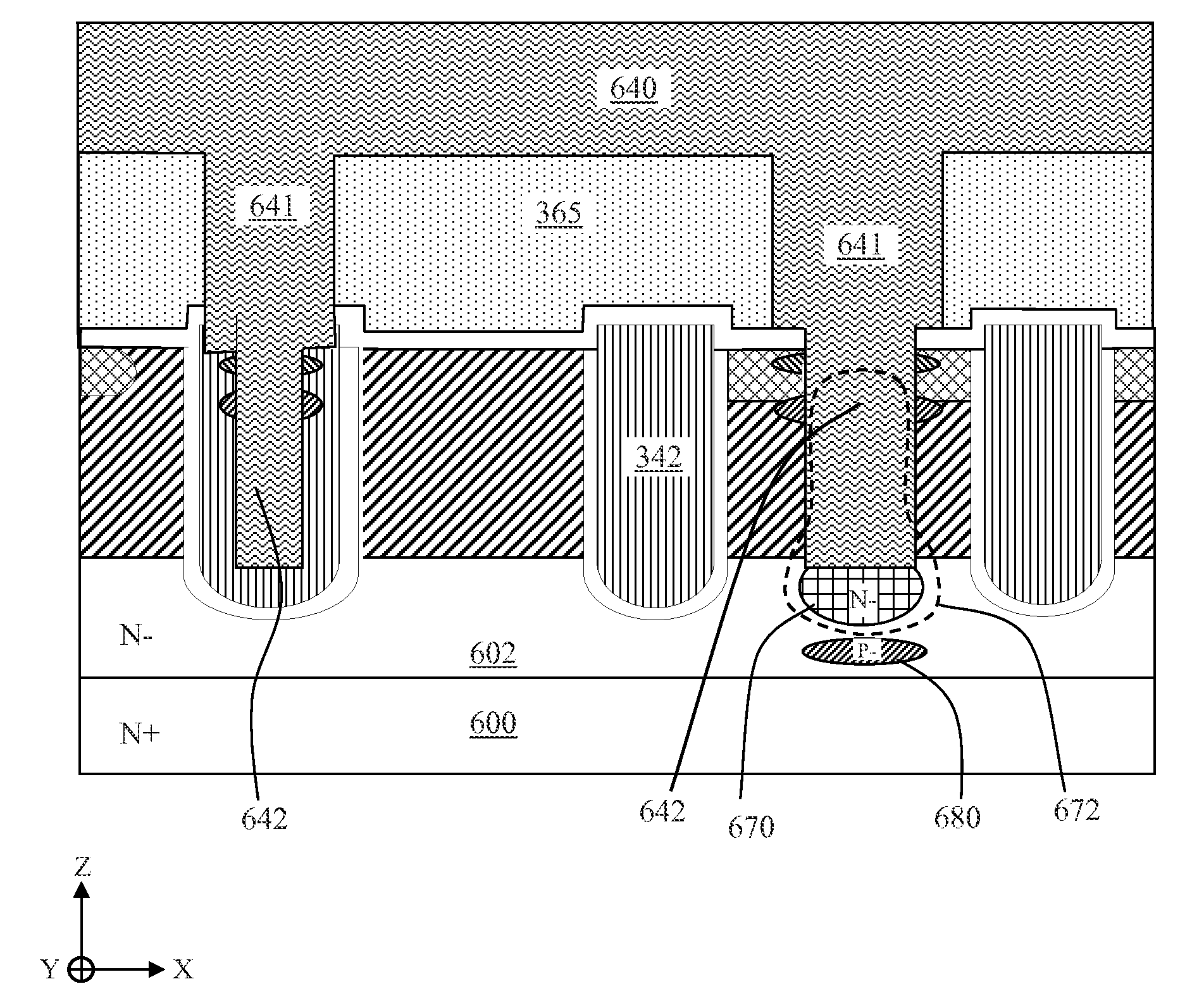
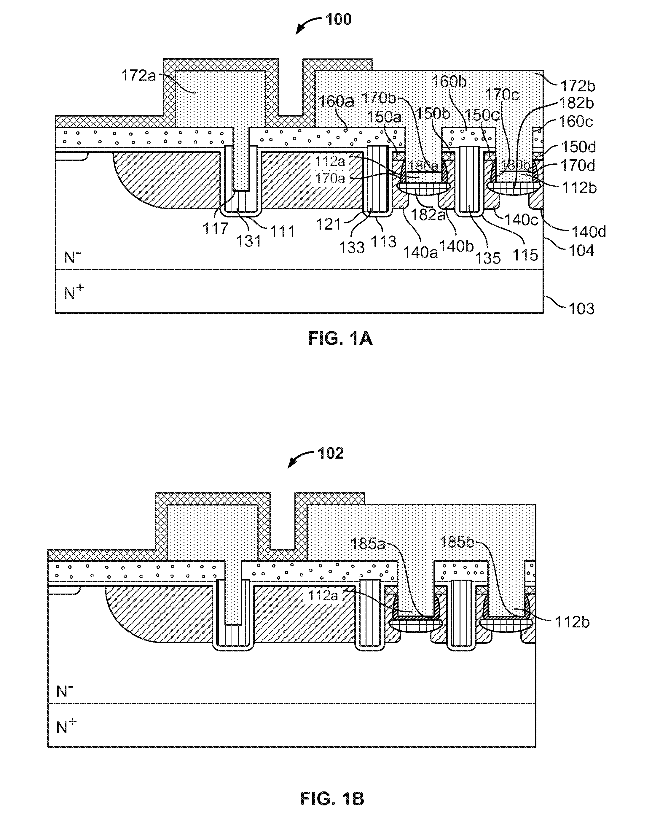
[0013]FIG. 1A is a cross-sectional diagram illustrating an embodiment of a double-diffused metal oxide semiconductor (DMOS) device with reduced breakdown voltage. In this example, device 100 includes a drain that is formed on the back of an N+-type semiconductor substrate 103. The drain region extends into an epitaxial (epi) layer 104 of N−-type semiconductor that overlays substrate 103...


PUM


Abstract

A MOSFET device and fabrication method are disclosed. The MOSFET has a drain in chip plane with an epitaxial layer overlay atop. The MOSFET further comprises: a Kelvin-contact body and an embedded Kelvin-contact source; a trench gate extending into the epitaxial layer; a lower contact trench extending through the Kelvin-contact source and at least part of the Kelvin-contact body defining respectively a vertical source-contact surface and a vertical body-contact surface; a patterned dielectric layer atop the Kelvin-contact source and the trench gate; a patterned top metal layer. As a result: a planar ledge is formed atop the Kelvin-contact source; the MOSFET device exhibits a lowered body Kelvin contact impedance and, owing to the presence of the planar ledge, a source Kelvin contact impedance that is lower than an otherwise MOSFET device without the planar ledge; and an integral parallel Schottky diode is also formed.

Description

CROSS REFERENCE TO RELATED APPLICATIONS[0001]This application is a Continuation-in-Part (CIP) of a commonly owned pending US application entitled “MOSFET device with reduced breakdown voltage”, Attorney Docket Number: ALPHP011, by Ji Pan and Anup Bhalla with application No. 12 / 317,629, filing date Dec. 23, 2008, by now published on Feb. 24, 2011 with publication number US20110042727.[0002]Whose content is herein incorporated by reference for any and all purposes.FIELD OF INVENTION[0003]This invention relates generally to the field of semiconductor device structure. More specifically, the present invention is directed to device structure and associated manufacturing method to form an integrated MOSFET Device with certain device performance parameters.BACKGROUND OF THE INVENTION[0004]Modern semiconductor devices, such as Metal Oxide Semiconductor Field Effect Transistors (MOSFETs) are often high density devices with small feature sizes. For example, the wall-to-wall pitch size of some...

Claims


Application Information

Patent Timeline
Patent Type & Authority Applications(United States)
IPC IPC(8): H01L29/78H01L21/336
CPCH01L29/0623H01L29/872H01L29/0878H01L29/1095H01L29/41766H01L29/4236H01L29/47H01L29/66128H01L29/66143H01L29/66719H01L29/66727H01L29/66734H01L29/7806H01L29/7811H01L29/7813H01L29/8611H01L29/086H01L21/26586H01L21/28238
Inventor PAN, JI
Owner ALPHA & OMEGA SEMICON INC
Why Eureka
Try Eureka