Display device and method of manufacture thereof

a technology of display device and display method, which is applied in the manufacture of electrode systems, electric discharge tubes/lamps, instruments, etc., can solve the problems of reduced brightness and contrast, large power consumption, and difficulty in achieving satisfactory image display, etc., and achieves high contrast, simple method, and high degree of reflection

Inactive Publication Date: 2012-03-22
PANASONIC CORP
View PDF6 Cites 32 Cited by
  • Summary
  • Abstract
  • Description
  • Claims
  • Application Information

AI Technical Summary

Benefits of technology

[0099](1) In the display device of the first aspect, the first electrode is provided independently in each pixel the bottom of the cell space facing the back substrate, and the second electrode is provided in the partition walls closer to the front substrate than the first electrode. Therefore, sufficient distance is guaranteed along the side of the partition walls between the second electrode and the outer periphery of the first electrode. When the driving unit applies driving voltage between the first electrode and the second electrode, electric energy density does not concentrate in a narrow region within the cell space. Rather, a uniform electrical field forms along the side of the partition walls between the second electrode and the outer periphery of the first electrode.
[0100]As a result, when displaying white, the colored particles enclosed in the cell space are caused to move to the side of the partition walls so as to evenly attach thereto, even with a relatively small the driving voltage. Therefore, this structure widely exposes pixels and achieves display with a high degree of reflection and high contrast.
[0101]Since the second electrode is at a common potential in all of the pixels, i.e. the second electrode is a

Problems solved by technology

Like transmissive type LCDs, however, OLEDs exhibit reduced brightness and contrast in direct sunlight, making it difficult to achieve satisfactory image display.
While the luminous efficiency of OLEDs has improved over recent years, considerable power consumption is required even when displaying black and white images, such as electronic book

Method used


Image

  • Display device and method of manufacture thereof
  • Display device and method of manufacture thereof
  • Display device and method of manufacture thereof

Examples


embodiment 1-1

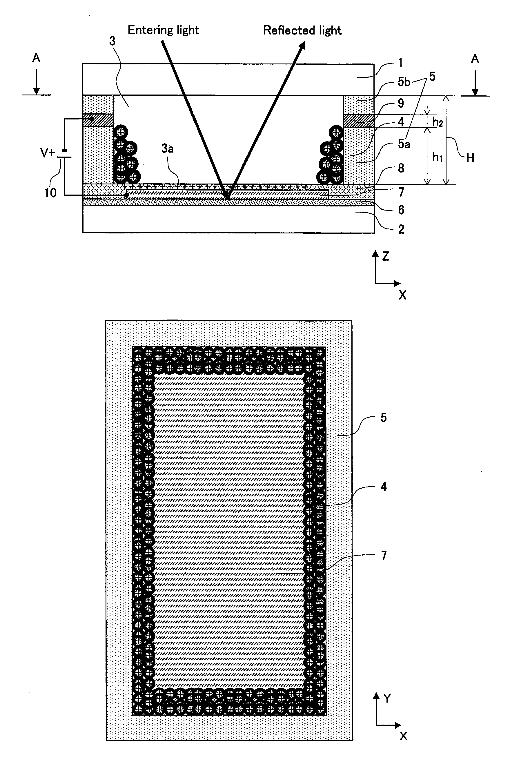
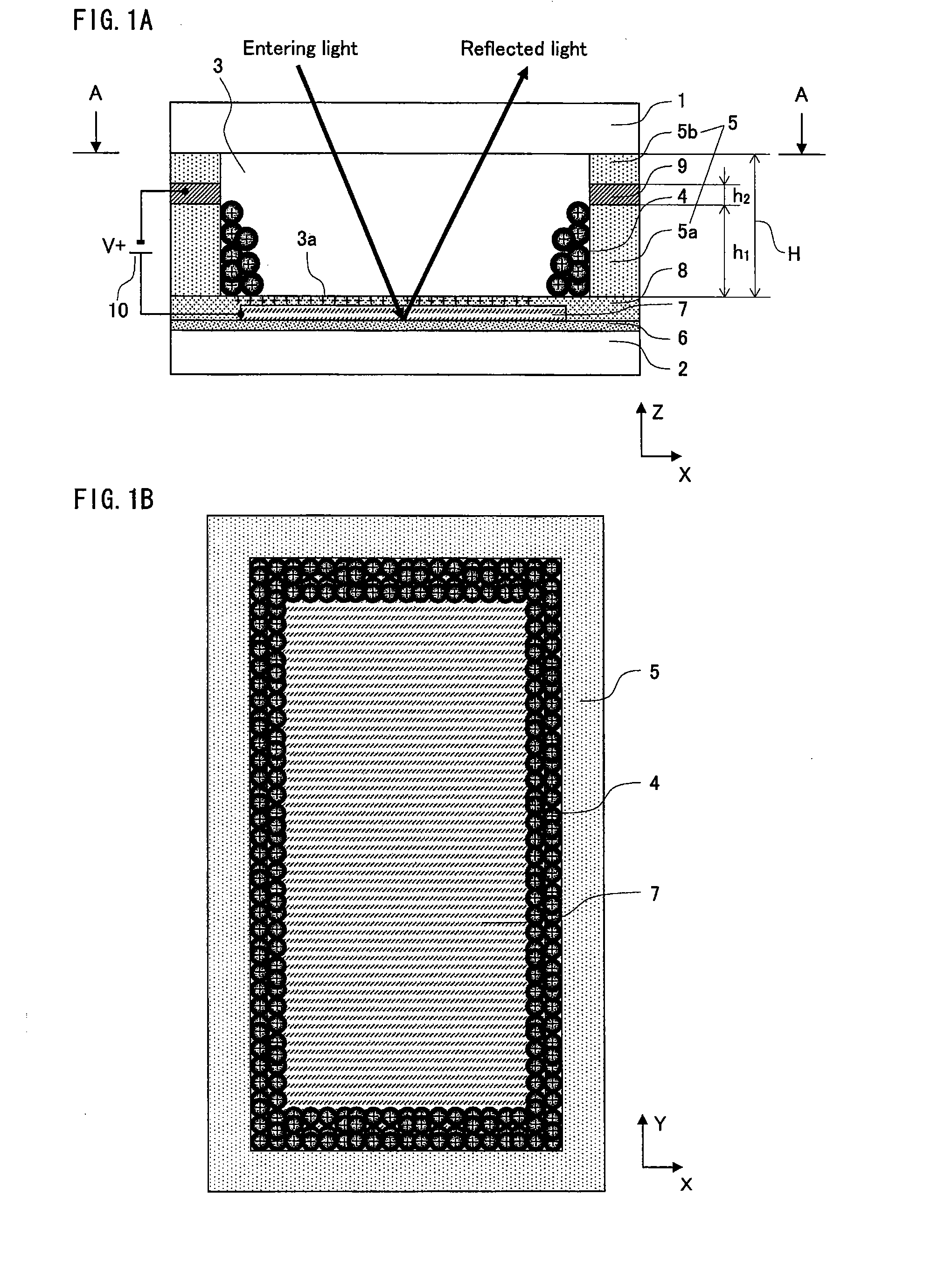
[0220]A display device according to the present embodiment is composed of a driving unit 10 and a display panel 100, in which a plurality of pixels are arranged in a matrix along the horizontal direction (X direction) and the vertical direction (Y direction).

[0221]The following describes the device structure of the display panel 100.

[0222]FIG. 1A is a partial cross-section diagram showing the structure of the display panel according to Embodiment 1-1, illustrating a representative pixel (unit of display).

[0223]The following describes a display panel in which each pixel displays black or white. A full-color display panel can also be achieved, however, by structuring each pixel to have sub-pixels that are red (R), green (G), and blue (B), or cyan (C), yellow (Y), and magenta (M).

[0224]An example of the size of each pixel is a pitch of 300 μm in both the horizontal direction (X direction) and vertical direction (Y direction). In the case of a full-color display, each of the red (R), gr...

example 1

[0288]The following describes an example of a method of manufacturing the display panel 100.

Manufacturing the Back Substrate 2

[0289]The white reflective layer 6, which is formed from a titanium oxide (titania) film, is coated, printed, cold sprayed, or the like on the back substrate 2, which is formed from alkalifree glass, so as to be formed on the surface necessary for image display, i.e. almost the entire surface of the substrate except for the peripheral portion thereof.

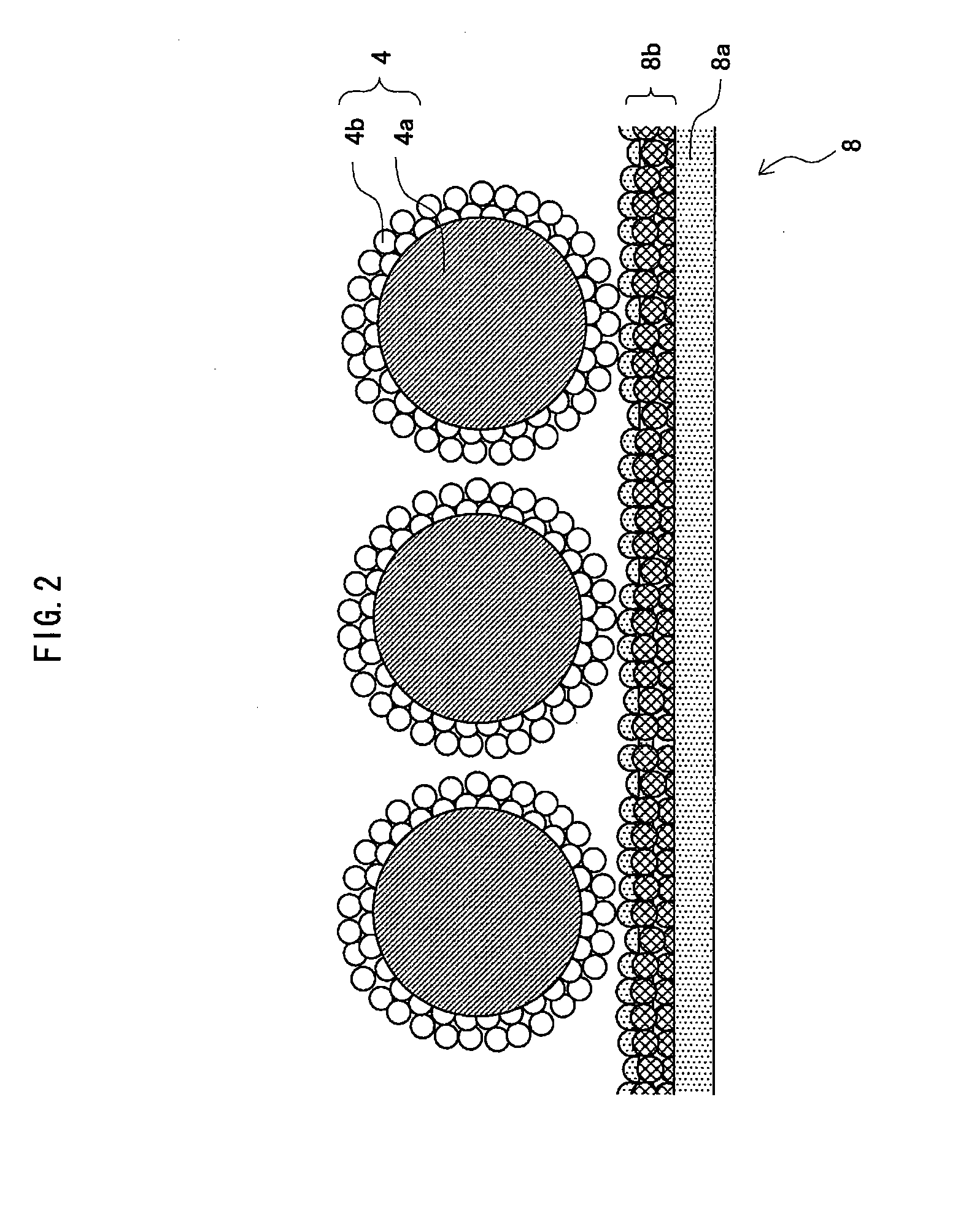
[0290]Next, a thin film is formed from ITO, which is a transparent conductive material, by sputtering, vapor deposition, or the like, and a predetermined rectangular shape is patterned by a process such as lithography or etching in order to form the first electrode 7. Polycarbonate charge transport material that is dissolved in a solvent is then coated or printed to form the insulating layer 8 on almost the entire substrate, except for the peripheral portion thereof. The surface-treated layer 8b, having protrusio...

modification to example 1

[0328]In Example 1 shown in FIG. 1, the dimensions of the first electrode 7 are set to fit within the region of the cell space 3 on the inner side of the partition walls 5. As in the example shown in FIG. 21, however, the first electrode 7 may be formed to extend beyond the region of the cell space 3, so that in plan view from the front of the panel, the outer periphery of the first electrode 7 overlaps the second electrode 9.

[0329]In this modification, as in the display panel 100 in FIG. 1, a uniform electrical field forms along the side of the partition walls 5. Since the electric energy density grows higher, however, the driving voltage may be lowered. This advantageous effect is similar to the advantageous effect of forming the second electrode 9 to project from the side of the partition walls 5 as described below in Embodiment 1-2.


PUM


Abstract

Disclosed is a paper-like display device which has improved contrast and image quality and is capable of high-speed operation. A front substrate 1 and a back substrate 2 are disposed to face each other with a space therebetween, and the space is partitioned by partition walls 5 in the vertical (Y) direction and the horizontal (X) direction in a crisscrossed fashion into cell spaces 3. A predetermined quantity of black-colored particles 4 is enclosed within each cell space 3. A white reflective layer 6, first electrodes 7, and an insulating layer 8 are formed on the inner surface of the back substrate 2. Each first electrode 7 is separately formed for a different pixel and extends along the bottom surface of the cell space 3. Each partition wall 5 includes an upper partition wall 5b, facing the front substrate 1, and a lower partition wall 5a, facing the back substrate 2. A second electrode 9 serving as a common electrode is formed between the upper partition wall 5b and the lower partition wall 5a.

Description

TECHNICAL FIELD[0001]The present invention relates to display devices that display images, and in particular to display devices such as electronic paper that display images through movement of colored particles between electrodes.BACKGROUND ART[0002]In recent years, a variety of mobile devices, starting with cellular telephones, have become widespread. At the same time, development of displays used in these devices has progressed rapidly. In addition to liquid crystal displays (LCDs) and organic electroluminescent displays (OLEDs), electronic paper has also emerged on the market.[0003]These display devices include a display panel having pixels arranged in a matrix on a substrate, the pixels being composed of display elements such as EL elements, liquid crystal elements, electronic paper, or the like. The display devices also include a driving means that applies voltage to the display elements. Display characteristics differ depending on the type of display elements forming the pixel...

Claims


Application Information

Patent Timeline
IPC IPC(8): G06F3/038H01J9/00G02F1/1677
CPCG02F1/167G02F2001/1672H01L27/3244H01L27/3232G02F2001/1674G02F1/1681G02F1/1671G02F1/1677H10K59/50H10K59/12G09G5/10
Inventor YAMAKITA, HIROYUKI
Owner PANASONIC CORP
Why Eureka
Try Eureka