Photoelectric Conversion Device and Image Pick-Up Device

a technology of photoelectric conversion and image pickup, which is applied in the direction of selective content distribution, radio control devices, television systems, etc., can solve the problems of unnecessary current generation and image quality deterioration, and achieve the effects of preventing image quality deterioration, reducing size, and reducing the level of pixel signals

Active Publication Date: 2012-04-12
ROHM CO LTD
View PDF7 Cites 65 Cited by
  • Summary
  • Abstract
  • Description
  • Claims
  • Application Information

AI Technical Summary

Benefits of technology

[0030]Since first and second planar electrodes forming a capacitor are provided in the insulating layer under the photoelectric conversion film in the photoelectric conversion device according to the present invention, deterioration of image quality can be prevented by cutting off light incident on a semiconductor substrate and reduction in size can be achieved.
[0031]In another photoelectric conversion device according to the present invention, a first pixel signal is generated during the first period based on a voltage of the second capacitor while an output current from the photoelectric conversion element is fed t

Problems solved by technology

When light is incident on a transistor provided around the photoelectric conversion portion on the

Method used


Image

  • Photoelectric Conversion Device and Image Pick-Up Device
  • Photoelectric Conversion Device and Image Pick-Up Device
  • Photoelectric Conversion Device and Image Pick-Up Device

Examples


embodiment 1

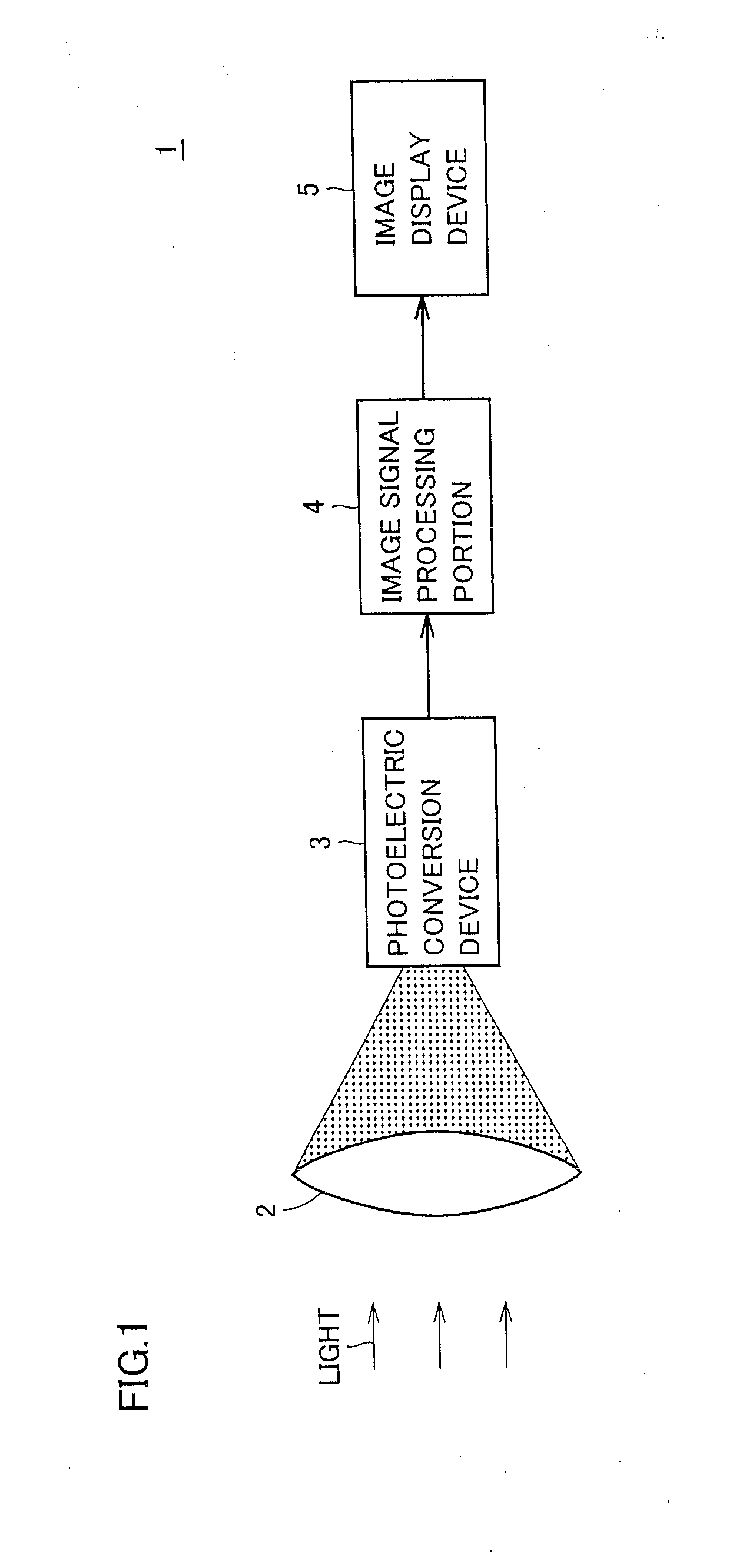
[0117]FIG. 1 is a diagram showing a configuration of an image pick-up device 1 according to Embodiment 1 of the present invention.

[0118]Referring to FIG. 1, image pick-up device 1 includes a lens 2, a photoelectric conversion device 3, an image signal processing portion 4, and an image display device 5.

[0119]Image pick-up device 1 picks up an image of a subject and displays the picked-up image on a screen. More specifically, lens 2 condenses light from the subject on photoelectric conversion device 3. Photoelectric conversion device 3 converts light received from lens 2 to a pixel signal which is an electric signal and outputs the pixel signal to image signal processing portion 4. Image signal processing portion 4 generates an image signal by subjecting a pixel signal of each pixel received from photoelectric conversion device 3 to various types of signal processing such as interpolation processing, color processing and correction processing, and outputs the image signal to image di...

embodiment 2

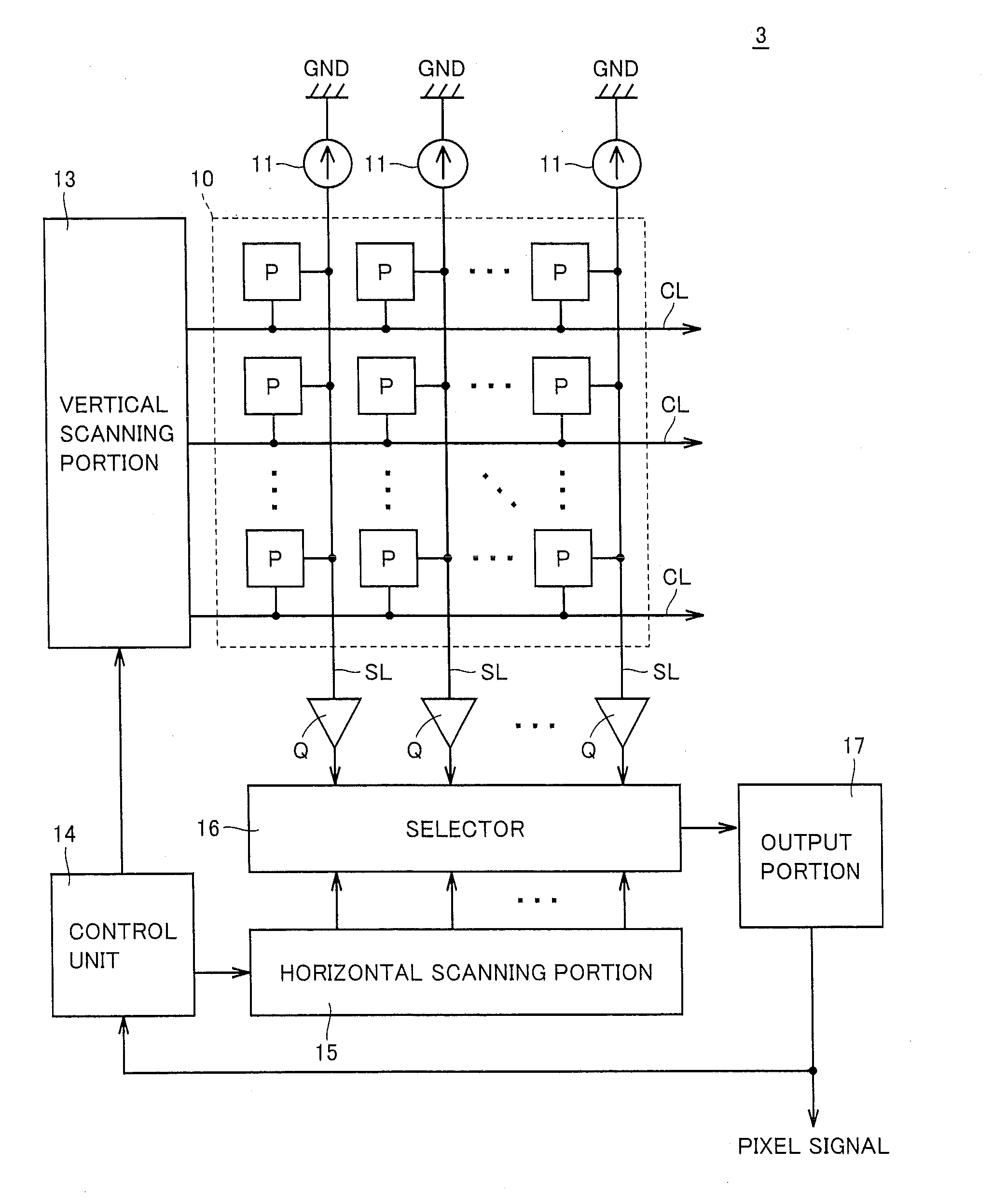
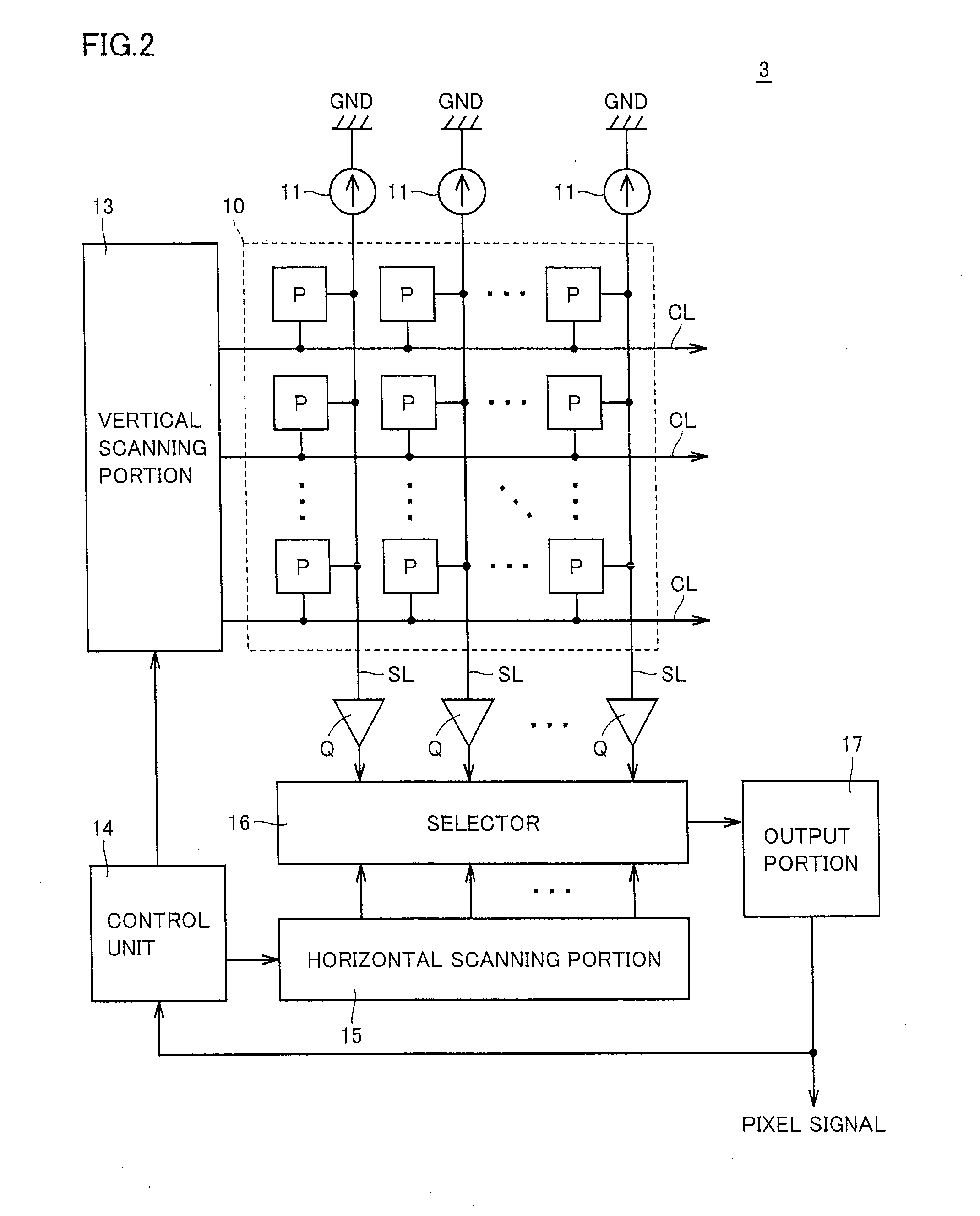
[0171]A photoelectric conversion device according to Embodiment 2 of the present invention includes a pixel array 26 as shown in FIG. 10. Pixel array 26 includes m×n pixels P11 to Pmn aligned in m rows and n columns (each of m and n being an integer not smaller than 2), control signal line groups CL1 to CLm provided in correspondence with m rows respectively, and signal lines SL1 to SLn provided in correspondence with n columns respectively. Pixel P is controlled by a plurality of signals provided through corresponding control signal line group CL, and it successively outputs to corresponding signal line SL, a pixel current at a level in accordance with a quantity of incident light and a reference current corresponding to a pixel current in a case where a quantity of incident light is zero.

[0172]One end of each signal line SL is connected to a line of ground voltage GND through load circuit 11. Load circuit 11 has a prescribed resistance value. The other end of each signal line SL i...

embodiment 3

[0223]An ordinary CMOS image sensor includes, for example, a plurality of photoelectric conversion elements and a plurality of amplifiers provided in correspondence with the respective photoelectric conversion elements, each for amplifying charges from a corresponding photoelectric conversion element. Then, a good image is obtained even when illuminance is low, by using an output from each amplifier for generating a pixel signal in normal condition and using combined outputs from the amplifiers for generating a pixel signal when illuminance is low. Namely, as signals and noises are added by combining outputs from the amplifiers, the signals are multiplied and the noise increases by root mean square. Therefore, an S / N (Signal to Noise) ratio of a pixel signal is improved. Such a method is adopted also in a CCD (Charge Coupled Device) image sensor.

[0224]Such a method, however, has been disadvantageous in that an effect of improvement in the S / N ratio of a pixel signal is low and signi...


PUM


Abstract

A photoelectric conversion device includes a semiconductor substrate, an insulating layer provided on the semiconductor substrate, an electrode provided on the insulating layer, a photoelectric conversion film provided on the electrode for converting received light to charges, a line connected between the electrode and the semiconductor substrate, a first planar electrode provided in the insulating layer and connected to the electrode, and a second planar electrode provided in the insulating layer between the first planar electrode and the semiconductor substrate.

Description

TECHNICAL FIELD[0001]The present invention relates to a photoelectric conversion device and an image pick-up device, and particularly to a photoelectric conversion device and an image pick-up device including a photoelectric conversion film.BACKGROUND ART[0002]In a solid-state image sensing element employed in a CMOS (Complementary Metal Oxide Semiconductor) image sensor or the like, for example, a photoelectric conversion portion is provided on a silicon substrate and light should pass through as far as a substrate surface. When light is incident on a transistor provided around the photoelectric conversion portion on the silicon substrate, however, an unnecessary current is generated and image quality may deteriorate.[0003]As a technique for preventing disadvantages caused by incident light, for example, Japanese Patent Laying-Open No. 2004-140309 (PTL 1) discloses the following solid-state image sensing element. Namely, a photoelectric conversion element generating and storing cha...

Claims


Application Information

Patent Timeline
IPC IPC(8): H01L31/0232H01L31/14H01L31/0224
CPCH01L27/14603H01L27/14609H01L27/14621H01L27/14623H01L31/0322H01L27/14632H01L27/14643H01L27/14685H01L27/14696H01L27/14627H01L27/14665H04N25/585H04N25/70H04N25/133H04N25/135G06F16/435H04N25/75H04N23/54H04N25/745H01L27/14658H04N5/33H04N9/646H04N21/2543H04N21/25866H04N21/25891H04N21/2743H04N21/278H04N21/4223H04N21/4532H04N21/458H04N21/47205H04N21/4756H04N21/4758H04N21/4828H04N21/812H04N21/854
Inventor NISHIYAMA, HIROSHIESUMI, TAKASHI
Owner ROHM CO LTD
Why Eureka
Try Eureka