

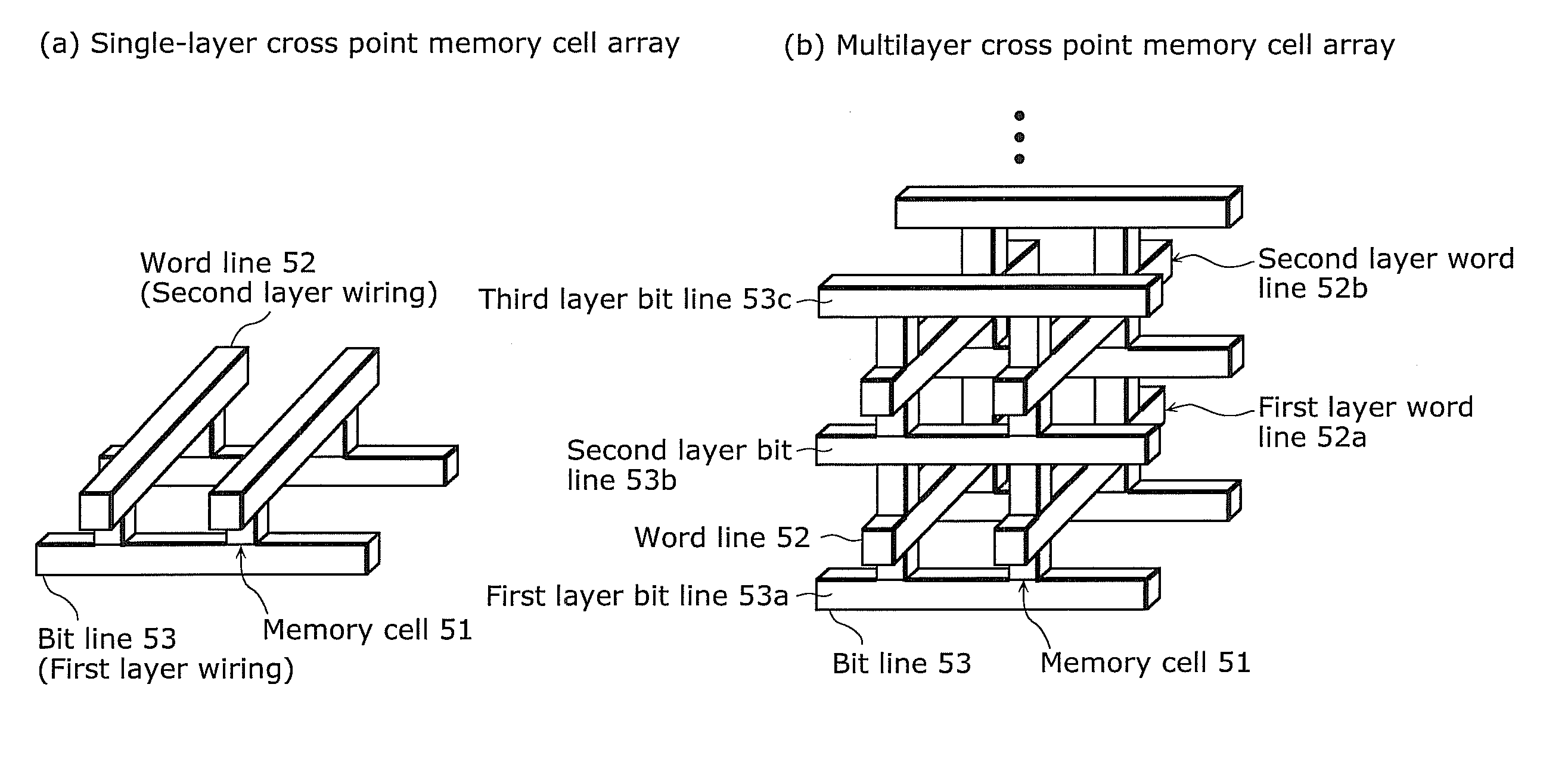
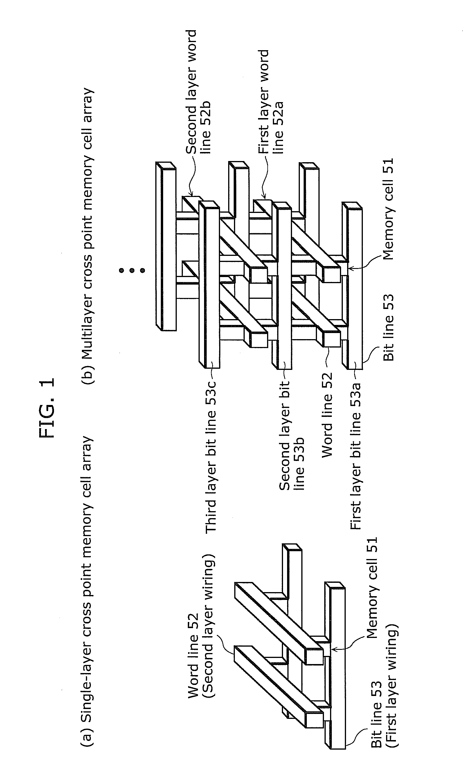
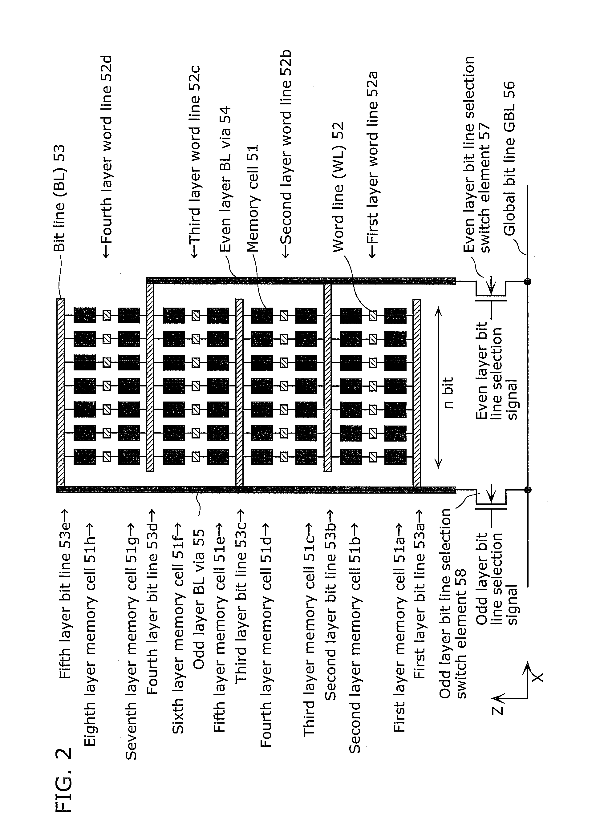
Cross point variable resistance nonvolatile memory device
a non-volatile, cross-point variable technology, applied in semiconductor devices, digital storage, instruments, etc., can solve the problems of inability to perform stable resistance change operation in odd layer memory cells, and achieve stable writing operation and easy manufacturing
- Summary
- Abstract
- Description
- Claims
- Application Information
AI Technical Summary
Benefits of technology
Problems solved by technology
Method used
Image

Examples
embodiment 1
[Description of Circuit Structure According to Present Invention]
[0120]FIG. 10 is a diagram showing a cross section structure of a memory cell 51 included in a cross point variable resistance nonvolatile memory device having a multilayer memory cell array in an embodiment of the present invention.
[0121]The memory cell 51 has a structure in which a first electrode 23 comprising tantalum nitride (TaN), a current steering layer 22 comprising nitrogen-deficient silicon nitride, a second electrode 21 comprising TaN, a first variable resistance layer 13 comprising oxygen-deficient tantalum oxide (TaOx), a second variable resistance layer 12 formed by oxidation of the first variable resistance layer 13 in an oxygen plasma atmosphere and comprising TaOy (xx, and a third electrode 11 comprising platinum (Pt) are stacked in this order. A lower wire 71 comprising aluminum (Al) is disposed below the memory cell 51, and connected to the first electrode 23 of the memory cell 51 by a first via 28....
example 1
[0191]As an operation of writing the multilayer cross point variable resistance nonvolatile memory device in Example 1, the following describes an operation whereby, when performing low resistance writing to a selected memory cell depending on a memory cell layer to which the selected memory cell belongs to, low resistance writing is performed by activating only one of the N-type current limiting element 90 and the P-type current limiting element 91 that has a higher substrate bias effect, with the source follower mode being used for current limitation in low resistance writing. The saturation current limiting mode will be described in detail later as Embodiment 2.
[0192]Table 1 shows set voltages of main signals in the diagram of the basic structure shown in FIG. 11 in association with each of the operations of the memory cells M1 to M4 of the different layers, in the source follower mode. In the table, “(ON: SF)” means that the current limiting element is ON and the source follower...
embodiment 2
[0342]In Embodiment 1, in the operation of writing to the multilayer cross point nonvolatile memory device, only one transistor out of the N-type current limiting element 90 and the P-type current limiting element 91 that has a higher substrate bias effect in a direction in which a current for low resistance writing flows through the memory cell is activated depending on the writing target memory array layer to which the memory cell belongs, to thereby perform the low resistance writing operation. In such low resistance writing, the current flow is limited in the source follower operation mode (i.e. the source follower mode).
[0343]Embodiment 2 is based on the same structure in which the N-type current limiting element 90 and the P-type current limiting element 91 are included, but differs in control method. Depending on the writing target memory array layer, a desired gate voltage is applied to the gate terminal of each of the N-type current limiting element 90 and the P-type curren...
PUM
 Abstract
Description
Claims
Application Information