Power module using sintering die attach and manufacturing method thereof

a technology of power modules and dies, applied in the direction of machine/engine, manufacturing tools, machine/engine, etc., can solve the problems of low reliability of materials, low efficiency of existing chip bonding methods, and difficulty in applying high-power electrical device modules to achieve the effect of excellent radiation characteristics and high electrical efficiency

Inactive Publication Date: 2012-05-03
SAMSUNG ELECTRO MECHANICS CO LTD
View PDF9 Cites 30 Cited by
  • Summary
  • Abstract
  • Description
  • Claims
  • Application Information

AI Technical Summary

Benefits of technology

[0011]The present invention has been made in an effort to provide a power module using sintering die attach having high electrical efficiency and excellent radiation characteristics, and a manufacturing method of the same.

Problems solved by technology

However, the existing chip bonding method has difficulties in being applied to a high-power electrical device module due to tin (Sn)-based low thermal conductivity (<60 W / m.k), formation of an inter metallic contact (IMC), and low reliability of a material itself.
In addition, the existing chip bonding method also has a problem of degradation in efficiency due to low radiation characteristics.
If cracks occur in the lower portion of the chip due to long use of the power module, it leads to degradation in radiation characteristics and as a result, it also leads to malfunction of the device, thereby causing economic loss.

Method used


Image

  • Power module using sintering die attach and manufacturing method thereof
  • Power module using sintering die attach and manufacturing method thereof
  • Power module using sintering die attach and manufacturing method thereof

Examples


Embodiment Construction

[0030]Various objects, advantages and features of the invention will become apparent from the following description of embodiments with reference to the accompanying drawings.

[0031]The terms and words used in the present specification and claims should not be interpreted as being limited to typical meanings or dictionary definitions, but should be interpreted as having meanings and concepts relevant to the technical scope of the present invention based on the rule according to which an inventor can appropriately define the concept of the term to describe most appropriately the best method he or she knows for carrying out the invention.

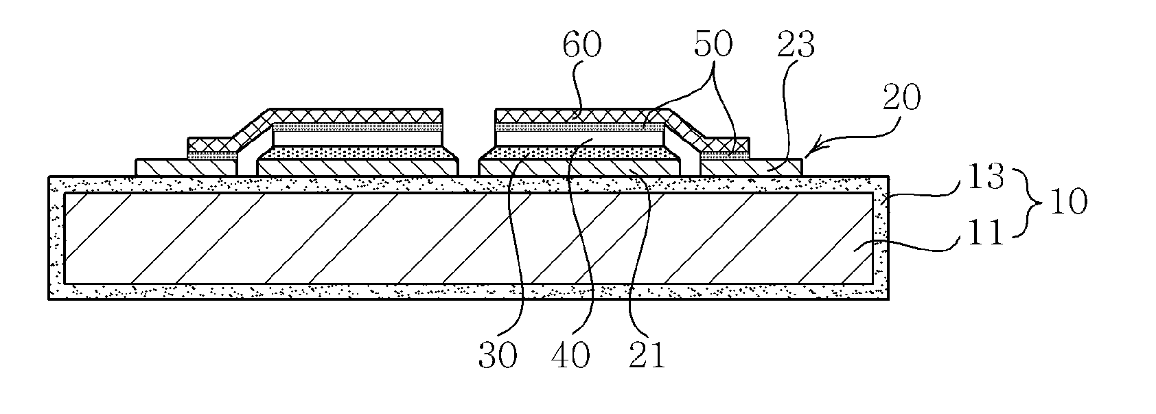
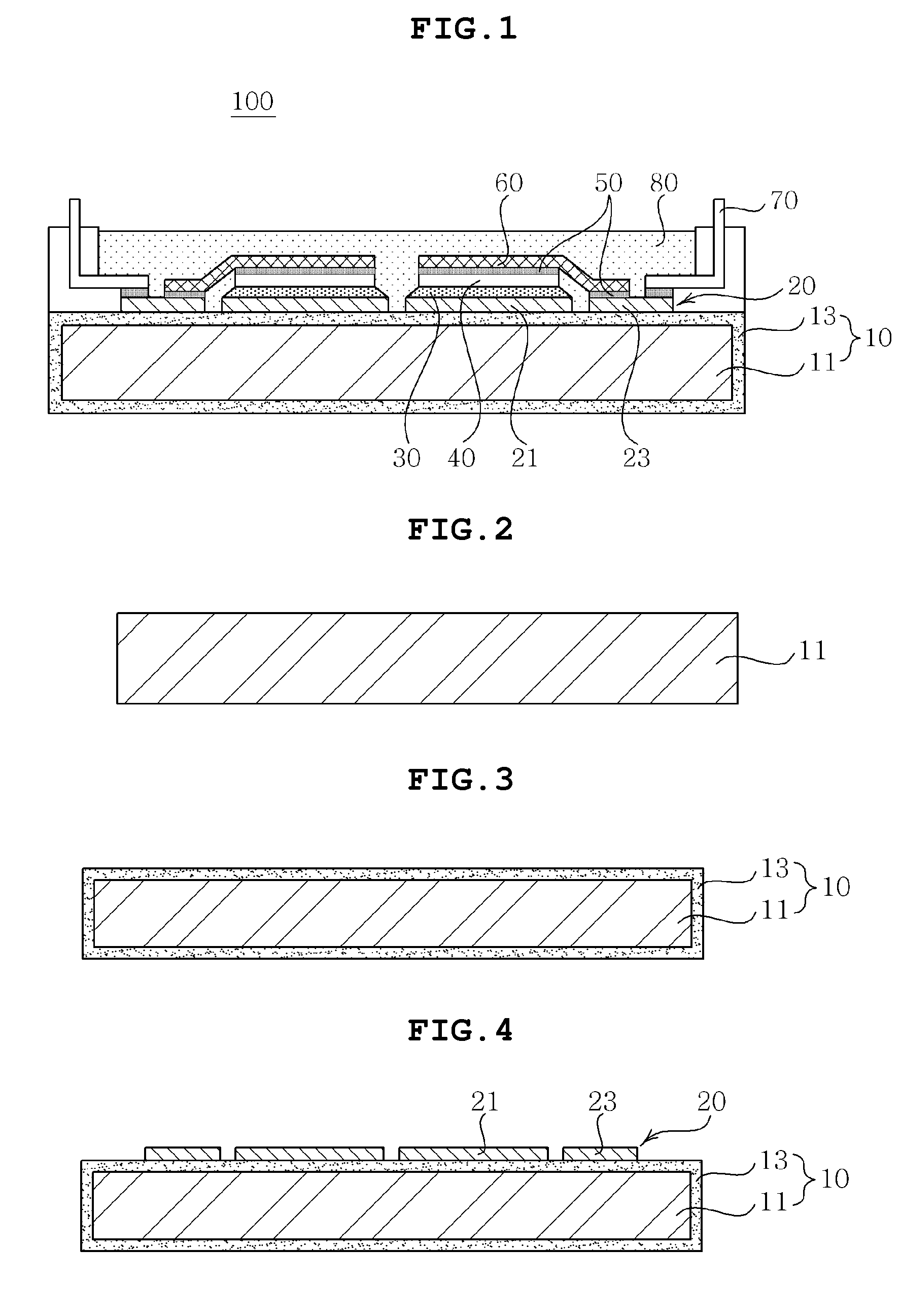
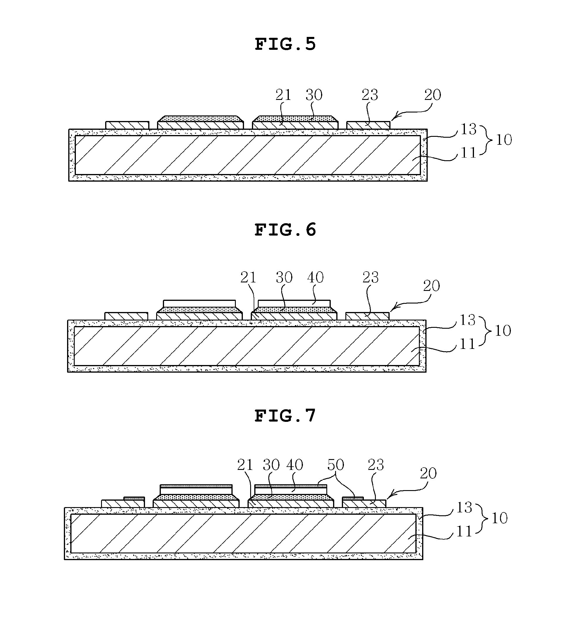
[0032]The above and other objects, features and advantages of the present invention will be more clearly understood from the following detailed description taken in conjunction with the accompanying drawings. In the specification, in adding reference numerals to components throughout the drawings, it is to be noted that like reference numerals designat...


PUM

PropertyMeasurementUnit
thicknessaaaaaaaaaa
temperatureaaaaaaaaaa
thicknessaaaaaaaaaa

Abstract

Disclosed herein are a power module using sintering die attach and a manufacturing method of the same. The power module includes: a substrate having an insulating layer formed on a surface of a metal plate; a circuit layer formed on the substrate and including a wiring pattern and an electrode pattern; a device mounted on the wiring pattern; a sintering die attach layer applying a metal paste between the wiring pattern and the device and sintering the metal paste to bond the wiring pattern to the device; and a lead frame electrically connecting the device to the electrode pattern, whereby making it possible to to simplify and facilitate the process, increase electrical efficiency and improve radiation characteristics, and manufacture firm and reliable power module.

Description

CROSS REFERENCE TO RELATED APPLICATION[0001]This application claims the benefit of Korean Patent Application No. 10-2010-0108340, filed on Nov. 2, 2010, entitled “Power Module Using Sintering Die Attach And Manufacturing Method Thereof”, which is hereby incorporated by reference in its entirety into this application.BACKGROUND OF THE INVENTION[0002]1. Technical Field[0003]The present invention relates to a power module using sintering die attach and a manufacturing method thereof.[0004]2. Description of the Related Art[0005]An existing power module was manufactured by bonding an insulated gate bipolar transistor (IGBT), a diode chip and the like to a copper (Cu) lead frame or a direct bonding Cu (DBC) substrate and electrically connecting between the substrate and the housing by an aluminum (Al) wire bonding method.[0006]At this time, the chip is bonded to the substrate using Sn-based solder. Therefore, the lower portions of the IGBT and the diode chip are made of metal such as silv...

Claims


Application Information

Patent Timeline
Patent Type & Authority Applications(United States)
IPC IPC(8): H05K7/02B23K31/02B23K1/20
CPCH01L23/3735H01L2224/8385H01L2224/8384H01L24/29H01L24/32H01L24/33H01L24/83H01L2224/291H01L2224/33181H01L2224/83193H01L2224/83801H01L25/072H01L2224/84801H01L2224/40095H01L24/40H01L24/36H01L2224/40225H01L2924/181H01L2224/83192H01L2924/1305H01L2924/15747H01L2924/00014H01L2224/29355H01L2224/29347H01L2224/29344H01L2224/29339H01L2224/29309H01L2224/29366H01L2224/45124H01L2224/32245H01L2924/00013H01L2924/01029H01L2924/13055H01L2224/29311H01L2924/014H01L2224/13099H01L2224/13599H01L2224/05599H01L2224/05099H01L2224/29099H01L2224/29599H01L2924/3512H01L2924/00H01L2224/48H01L2924/00012H01L2224/37099H01L24/84H01L2224/73221
Inventor KIM, TAE HYUNJOO, YONG HUICHOI, SEOG MOON
Owner SAMSUNG ELECTRO MECHANICS CO LTD
Why Eureka
Try Eureka