Semiconductor integrated circuit and operation method thereof

a technology of integrated circuits and semiconductors, applied in the direction of electric variable regulation, process and machine control, instruments, etc., can solve the problems of not being able to raise the output dc voltage v/sub>out above its limit, disadvantageous for obtaining constant current characteristics, etc., and achieve the effect of reducing the power consumption of the system

Active Publication Date: 2012-05-31
RENESAS ELECTRONICS CORP
View PDF6 Cites 51 Cited by
  • Summary
  • Abstract
  • Description
  • Claims
  • Application Information

AI Technical Summary

Benefits of technology

[0043]In the semiconductor integrated circuit 1 for the white LED array shown in FIG. 1, the level of the minimum voltage selected by the error amplifier 11 increases where the forward voltages VF of PN junctions of the LED devices D11 through D16, . . . , and D81 through D86 are reduced due the causes of a rise in temperature, variations in the characteristics of the LED devices, etc. Thus, the error amplifier 11 and the controller 12 of the step-up DC-DC converter 10 reduce the level of the output DC voltage VOUT in such a manner that the level of the increased and selected minimum voltage is reduced to the reference voltage VREF (=Vref+VSAT).
[0046]As a result, the values of the first channel LED drive current ILED<1> through the eighth channel LED drive current ILED<8> are lowered more than an initial normal constant current value. Thus, since a voltage drop developed across the constant current setting resistor Rs is significantly reduced more than the reference voltage Vref, the differential amplifier 211 and the N channel MOS transistor 212 of each driver unit 21 of the constant current driver 20 are operated to increase the reduced voltage drop developed across the constant current setting resistor Rs to the reference voltage Vref. That is, the differential amplifier 211 of the driver unit 21 supplies an extremely high level output voltage to the gate of the N channel MOS transistor 212 to compensate for the reduction in the first channel LED drive current ILED<1>.
[0051]It is thus an object of the present invention to provide a semiconductor integrated circuit for controlling and driving light emitting devices, which is capable of generating the optimum drive voltage even with respect to fluctuations in temperature and variations in the characteristics of the light emitting devices, etc. and reducing power consumption of a system.
[0063]According to the present invention, it is possible to generate the optimum drive voltage even with respect to fluctuations in temperature and variations in the characteristics of light emitting devices, etc. and thereby reduce power consumption of a system.

Problems solved by technology

Since, however, the switching regulator of FIG. 1 has a limit to a rise in the output DC voltage VOUT it is not possible to raise the level of the output DC voltage VOUT beyond its limit.
The MOS transistor 212 is operated in a linear region (a region in which a drain current changes substantially depending on the drain-to-source voltage) of the MOS transistor, which is disadvantageous for obtaining a constant current characteristic.

Method used


Image

  • Semiconductor integrated circuit and operation method thereof
  • Semiconductor integrated circuit and operation method thereof
  • Semiconductor integrated circuit and operation method thereof

Examples


first embodiment

[First Embodiment]

[0107]>

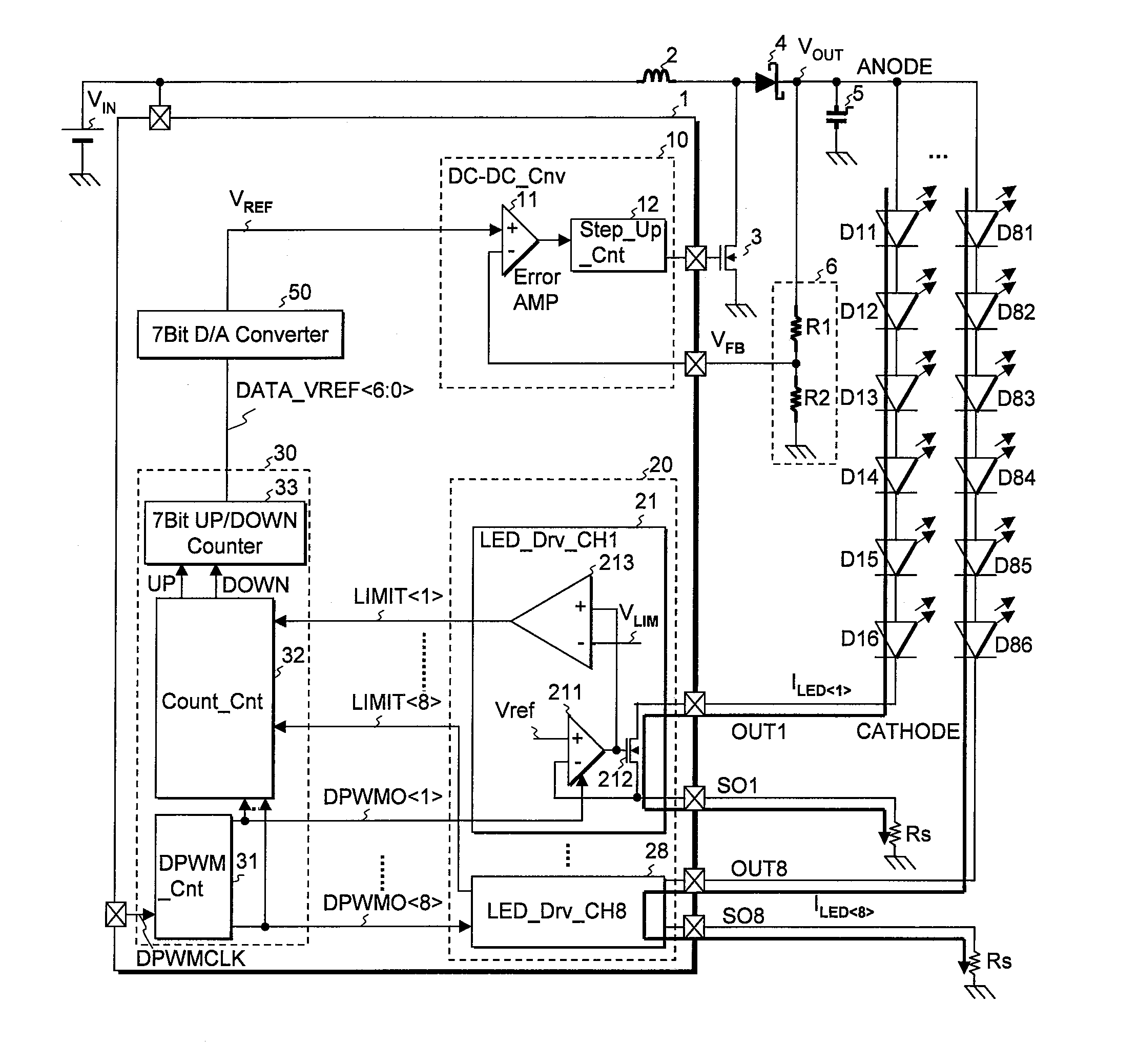
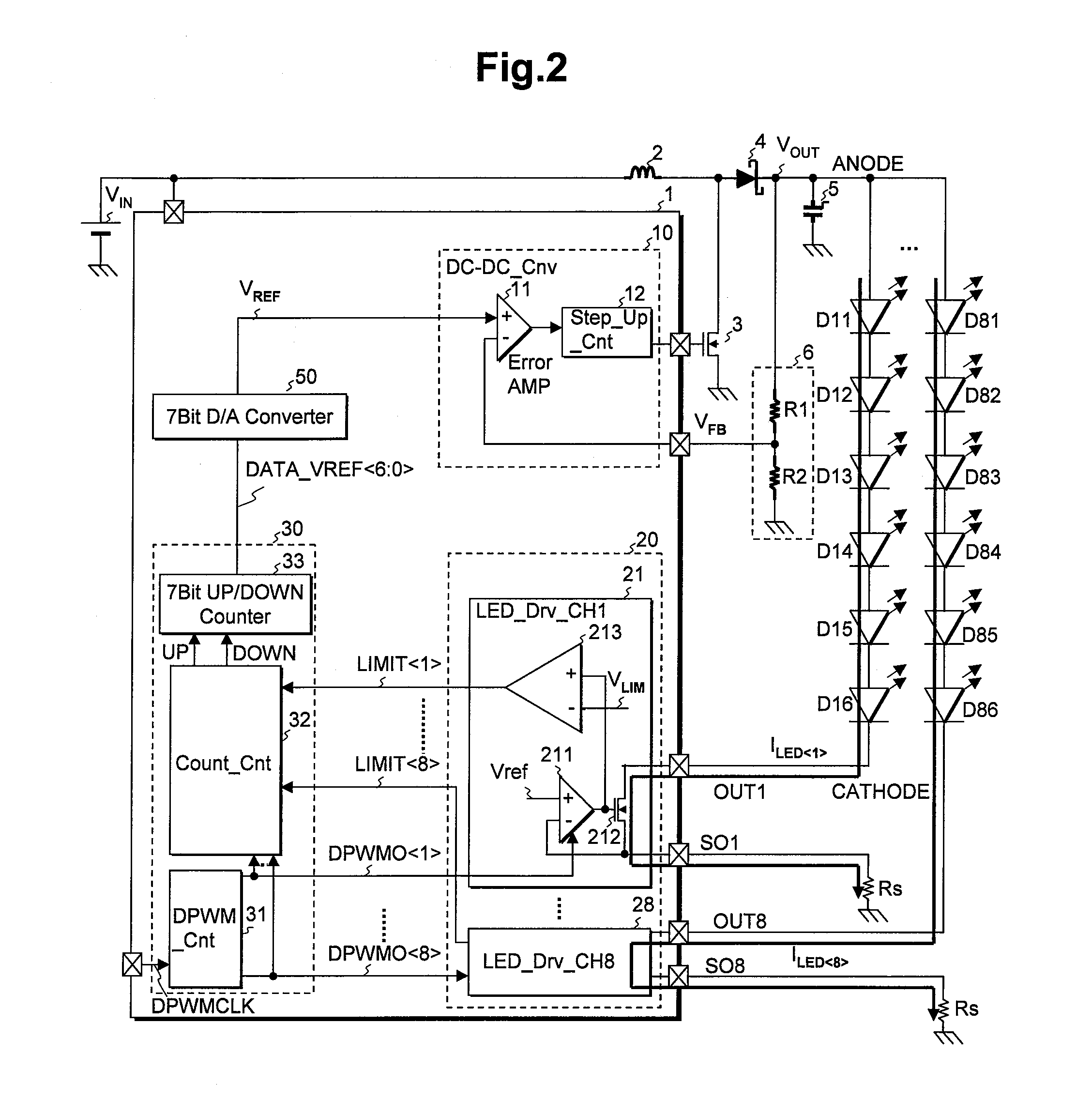
[0108]FIG. 2 is a diagram showing a configuration of a semiconductor integrated circuit for controlling and driving a white LED array, according to a first embodiment of the present invention.

[0109]The semiconductor integrated circuit 1 shown in FIG. 2 is comprised of a step-up DC-DC converter 10, a constant current driver 20 having eight channels (eight strings), a logic unit 30 and a reference voltage generation D / A converter 50. The logic unit 30 includes a 12-bit (4096-gradation) dimming controller 31, a counter controller 32 and an up / down counter 33. In the example of FIG. 2, for example, the DC-DC converter 10 is configured as a step-up DC-DC converter since an input DC voltage VIN is a relatively low voltage as in the case where its voltage range is from 10V to 26.0V. As another example, the DC-DC converter 10 is configured as a step-down DC-DC converter where the input DC voltage VIN is a relatively high voltage. As a further example, the DC-DC conv...

second embodiment

[0173]>

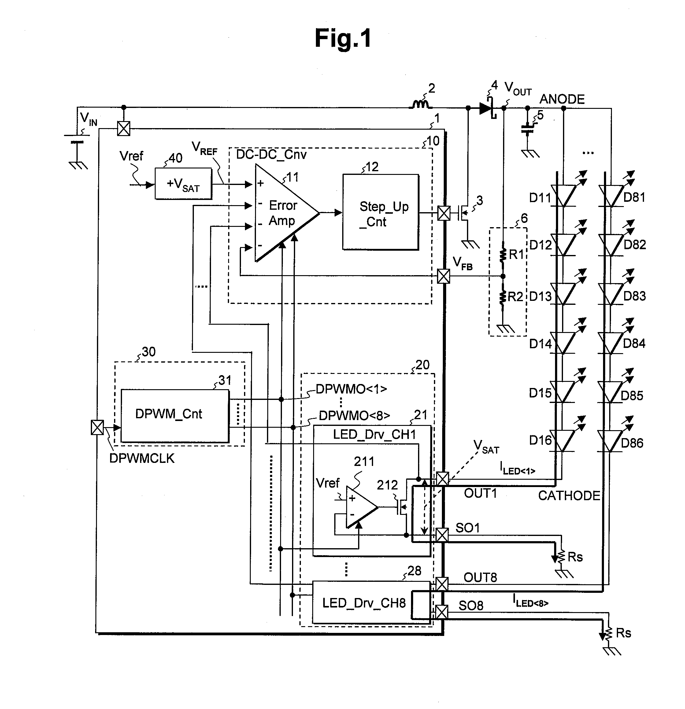
[0174]FIG. 5 is a diagram showing a processing flow of a calibration operation for an output DC voltage VOUT according to a second embodiment of the present invention, which is carried out in the semiconductor integrated circuit 1 of the present invention shown in FIG. 2.

[0175]At the first Step 500 of FIG. 5, the count value DATA_VREF6:0> of the up / down counter 33 is set to a predetermined initial value 3 Fh, and the low voltage find signal LOW_FIND indicative of first finding of the minimum voltage of the output DC voltage VOUT is set to a low level. The step-up controller 12 of the DC-DC converter 10 sets the reference voltage VREF corresponding to the initial value to 1.875V.

[0176]At the next Step 501, the counter controller 32 reads approximately in parallel, the levels of the abnormality detection determination signal LIMIT1> of the driver unit 21 through the abnormality detection determination signal LIMIT8> of the driver unit 28 for the eight channels in total. Actuall...

third embodiment

[0190]>

[0191]FIG. 6 is a diagram illustrating a configuration of a semiconductor integrated circuit for controlling and driving a white LED array, according to the third embodiment of the present invention.

[0192]The semiconductor integrated circuit 1 according to the third embodiment of the present invention shown in FIG. 6 is different in the following points from the semiconductor integrated circuit 1 according to the first embodiment of the present invention shown in FIG. 2.

[0193]That is, an inversion input terminal and a non-inversion input terminal of an abnormality detection comparator 213 of a driver unit 21 of a constant current driver 20 in the semiconductor integrated circuit 1 according to the third embodiment of the present invention shown in FIG. 6 are respectively supplied with a voltage (voltage at a constant current set terminal SO1 of the driver unit 21) at a source terminal of an N channel MOS transistor 212, and an abnormality detection criterion voltage VLIM. Inc...


PUM


Abstract

A DC-DC converter supplies an output voltage to a plurality of channels of a light emitting device array in common. A current driver has a plurality of driver units which drive the channels. Each of the driver units includes a drive transistor and a detector which detects an abnormality of a drive current. A logic unit generates digital data in response to a plurality of detection signals and supplies the same to a D / A converter. An analog reference voltage of the D / A converter is supplied to the DC-DC converter. The logic unit executes a calibration operation which determines digital data for setting the minimum output DC voltage at the normal operation of all the channels by sequential updating of the digital data.

Description

CROSS-REFERENCE TO RELATED APPLICATIONS[0001]The present application claims priority from Japanese patent application JP 2010-263226 filed on Nov. 26, 2010, the content of which is hereby incorporated by reference into this application.BACKGROUND[0002]The present invention relates to a semiconductor integrated circuit for controlling and driving light emitting devices and an operation method thereof, and particularly to a technology effective in generating the optimum drive voltage even with respect to fluctuations in temperature and variations in the characteristics of light emitting devices, etc, and reducing power consumption of a system.[0003]A light emitting diode (LED) is a semiconductor device which applies a voltage in its forward direction to thereby emit light. The principle of light emission or luminescence thereof utilizes an electro-luminescence (EL) effect. Organic EL (OLEDs: Organic light-emitting diodes) are also included in light emitting diodes.[0004]The light emit...

Claims


Application Information

Patent Timeline
Patent Type & Authority Applications(United States)
IPC IPC(8): H05B37/02
CPCH05B33/0812H05B33/0887H05B33/0815H05B45/395Y02B20/30H05B45/56H05B45/375H05B45/38Y02B20/00Y02B20/40H05B45/54
Inventor KITAGAWA, YUHEIMINAMI, KAZUYASU
Owner RENESAS ELECTRONICS CORP
Why Eureka
Try Eureka