Semiconductor device, active matrix substrate, and display device

a technology of active matrix substrate and semiconductor device, which is applied in semiconductor devices, instruments, optics, etc., can solve the problems of increasing the steps needed for fabrication, complex semiconductor device, and bulky device as a whole, and achieves the effect of reducing leakage current and facilitating fabrication

Inactive Publication Date: 2012-06-14
SHARP KK
View PDF4 Cites 30 Cited by
  • Summary
  • Abstract
  • Description
  • Claims
  • Application Information

AI Technical Summary

Benefits of technology

[0010]It is an object of the present invention to obtain a configuration of a semiconductor device that can achieve leakage current reduction and that can be fabricated easily, without making its structure complex or making the device bulky.
[0016]The above-described embodiment makes it possible to obtain a configuration of a semiconductor device that can achieve leakage current reduction and that can be fabricated easily, without making its structure complex or making the device bulky.

Problems solved by technology

With the configuration as disclosed in JP2002-57341A, however, the structure of the semiconductor device becomes complex, the device as a whole becomes bulky, and the steps needed for fabrication increase.
Further, in the case of the aforementioned configuration, it is necessary to form a contact hole excessively used for the bottom gate electrode.
This leads to a possibility that the base insulation film could be pierced, etc.

Method used


Image

  • Semiconductor device, active matrix substrate, and display device
  • Semiconductor device, active matrix substrate, and display device
  • Semiconductor device, active matrix substrate, and display device

Examples


embodiment 1

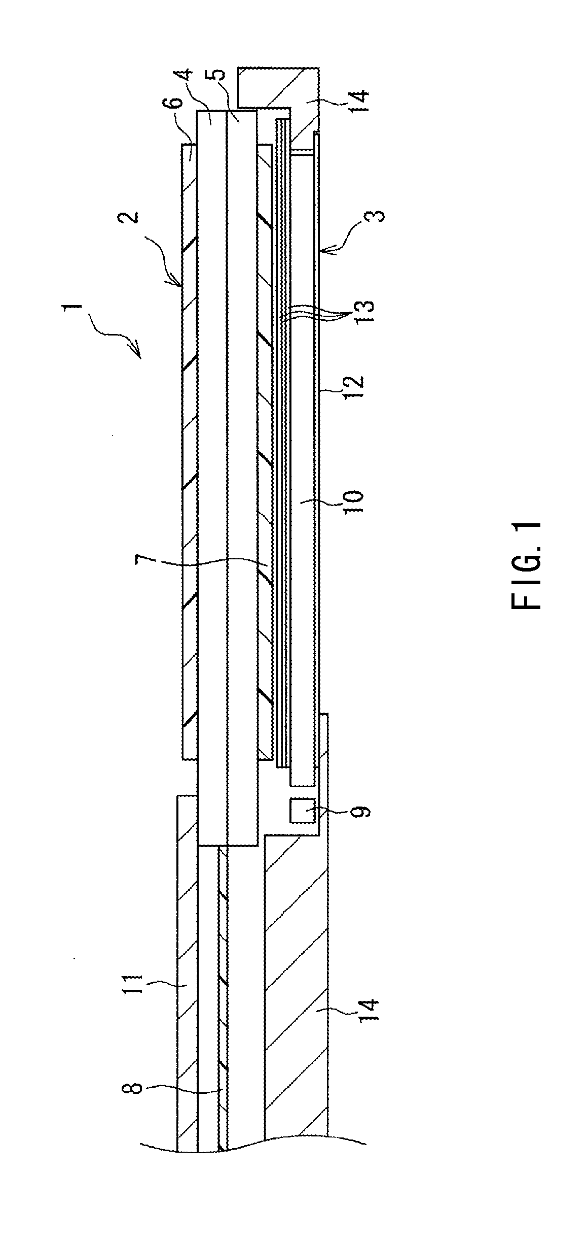
[0069]FIG. 1 is a cross-sectional view showing a configuration of a liquid crystal display device according to Embodiment 1. A liquid crystal display device 1 shown in FIG. 1 includes a liquid crystal panel 2 provided so that a viewed side thereof (display surface side) is the upper side as viewed in FIG. 1, and a backlight device 3 that is provided on a non-display surface side (lower side as viewed in FIG. 1) of the liquid crystal panel 2 and that irradiates the liquid crystal panel 2 with illumination light.

[0070]The liquid crystal panel 2 includes a color filter substrate 4 and an active matrix substrate 5 that composes a pair of substrates, and polarization plates 6 and 7 that are provided on outer side surfaces of the color filter substrate 4 and the active matrix substrate 5, respectively. Between the color filter substrate 4 and the active matrix substrate 5, a liquid crystal layer is interposed, though the illustration of the liquid crystal layer is omitted. A plate-like tr...

embodiment 2

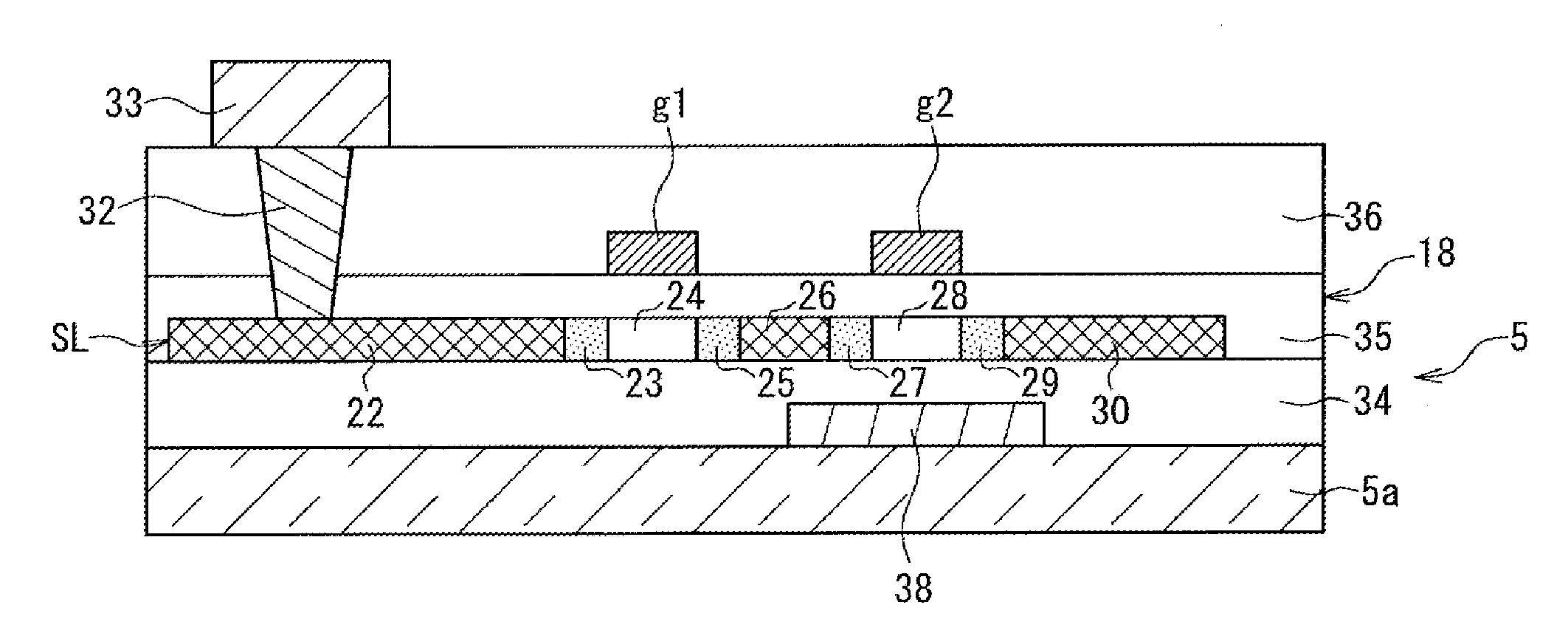
[0122]FIG. 8 is a plan view showing a schematic configuration of principal parts of a switching portion according to Embodiment 2. FIG. 9 is a cross-sectional view taken along a line IX-IX in FIG. 8. As shown in the drawings, the main difference of the present embodiment from embodiment 1 is that the bottom gate electrode is not rectangular in shape, but has a comb teeth shape. It should be noted that the elements in common with Embodiment 1 are denoted by the same reference numerals, and repetitive descriptions of the same are omitted.

[0123]More specifically, as shown in FIG. 8, in the switching portion 18 of the present embodiment, a bottom gate electrode 37 is formed in a comb teeth shape, and is provided below a carrier generation region where a light leakage current is generated (depleted region, i.e., a region in the vicinity of a drain junction part), which is a region in the silicon layer SL.

[0124]More specifically, as shown in FIG. 9, the bottom gate electrode 37 is divided...

embodiment 3

[0128]FIG. 10 is a circuit diagram showing an equivalent circuit of a switching portion according to embodiment 3. FIG. 11 is a plan view showing a schematic configuration of principal parts of the switching portion shown in FIG. 10. FIGS. 12(a) and 12(b) are cross-sectional views taken along lines XIIa-XIIa and XIIb-XIIb in FIG. 11, respectively. As shown in the drawings, the main difference of the present embodiment from Embodiment 1 is that a thin film transistor having only a top gate electrode (transistor with top gate structure) is connected in series to a thin film transistor having a top gate electrode (main gate electrode) and a bottom gate electrode (auxiliary gate electrode). It should be noted that the elements in common with Embodiment 1 are denoted by the same reference numerals, and repetitive descriptions of the same are omitted.

[0129]More specifically, as shown in FIG. 10, in the switching portion 18 of the present embodiment, a thin film transistor Tr1 having only ...


PUM


Abstract

Provided are a semiconductor device that can be fabricated easily and can achieve leakage current reduction, without its structure becoming complex or the device becoming bulky; an active matrix substrate in which the device is used; and a display device in which the device is used. A switching portion (18) (semiconductor device) provided with thin film transistors (Tr1, Tr2) having a top gate electrodes (g1, g2) (main gate electrodes) and a bottom gate electrode (21) (auxiliary gate electrode) includes a silicon layer (SL) (semiconductor layer) provided between the top gate electrodes (g1, g2) and the bottom gate electrode (21); and a light shielding film that shields a carrier generation region formed in the silicon layer from light. A potential of the top gate electrodes (g1, g2) is controlled by a gate signal supplied via a signal line, and a potential of the bottom gate electrode (21) is determined depending on capacity coupling between the bottom gate electrode (21) and the top gate electrodes (g1, g2).

Description

TECHNICAL FIELD[0001]The present invention relates to a semiconductor device provided with transistors, an active matrix substrate in which such a semiconductor device is used, and a display device in which such a semiconductor device is used.BACKGROUND ART[0002]Recently, a liquid crystal display device, for example, has been used as a flat panel display characterized in thinness, light weight, etc. as compared with a conventional cathode-ray tube, widely in liquid crystal televisions, monitors, portable telephones, etc. In such a liquid crystal display device, a plurality of data lines (source lines) and a plurality of scanning lines (gate lines) are arranged in matrix. Besides, the liquid crystal display device includes an active matrix substrate in which switching elements such as thin film transistors (hereinafter abbreviated as “TFT”) located in the vicinity of intersections between the data lines and the scanning lines, and pixels having pixel electrodes connected to the switc...

Claims


Application Information

Patent Timeline
Patent Type & Authority Applications(United States)
IPC IPC(8): H01L29/786
CPCG02F1/13624H01L29/42384H01L29/78648H01L29/78645H01L29/78633
Inventor KITAKADO, HIDEHITO
Owner SHARP KK
Why Eureka
Try Eureka