Silicon carbide epitaxial wafer and manufacturing method therefor

a technology of silicon carbide and epitaxial wafer, which is applied in the direction of crystal growth process, polycrystalline material growth, chemically reactive gas growth, etc., can solve the problems of sic or 8h, the performance improvement has reached a limit due to the limitations of material properties, and the different polytype of the substrate is easily contaminated

Active Publication Date: 2012-06-14
RESONAC CORP
View PDF1 Cites 34 Cited by
  • Summary
  • Abstract
  • Description
  • Claims
  • Application Information

AI Technical Summary

Benefits of technology

[0060]According to the above-described configuration, a

Problems solved by technology

Although improvements to power electronics have been made regarding the technical performance using related art silicon (Si) semiconductors, performance improvement has reached a limit due to limitations of the material properties of silicon.
In the epitaxial film, a polytype that is different from a polytype used in the substrate is easily contaminated, and for example, in the case of using 4H—SiC in the substrate, 3C—SiC

Method used


Image

  • Silicon carbide epitaxial wafer and manufacturing method therefor
  • Silicon carbide epitaxial wafer and manufacturing method therefor
  • Silicon carbide epitaxial wafer and manufacturing method therefor

Examples


embodiment 1

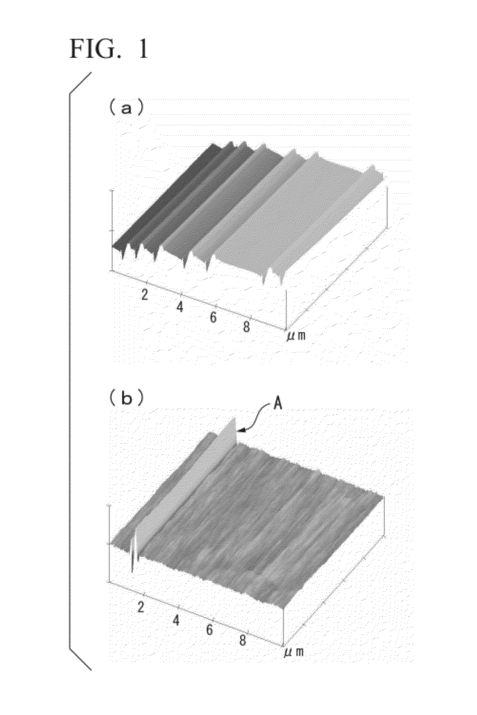
[0121]In the polishing process, abrasive particles having a diameter of 5 μm were used in performing mechanical polishing before CMP, and the processing pressure was 350 g / cm2. Further, the CMP was performed for 30 minutes using silica particles having an average particle diameter of 10 to 150 nm as abrasive particles, sulfate as an inorganic acid, and abrasive slurry having the pH of 1.9 at 20° C.

[0122]After RCA cleaning of the substrate after polishing, the substrate was introduced into a growth device. Further, the RCA cleaning is a wet cleaning method generally used with respect to the Si wafer, and can remove organics, heavy metals, and particles on the substrate surface using a solution in which sulfate, ammonia, hydrochloride, and hydrogen peroxide solution are mixed and a hydrofluoric acid solution.

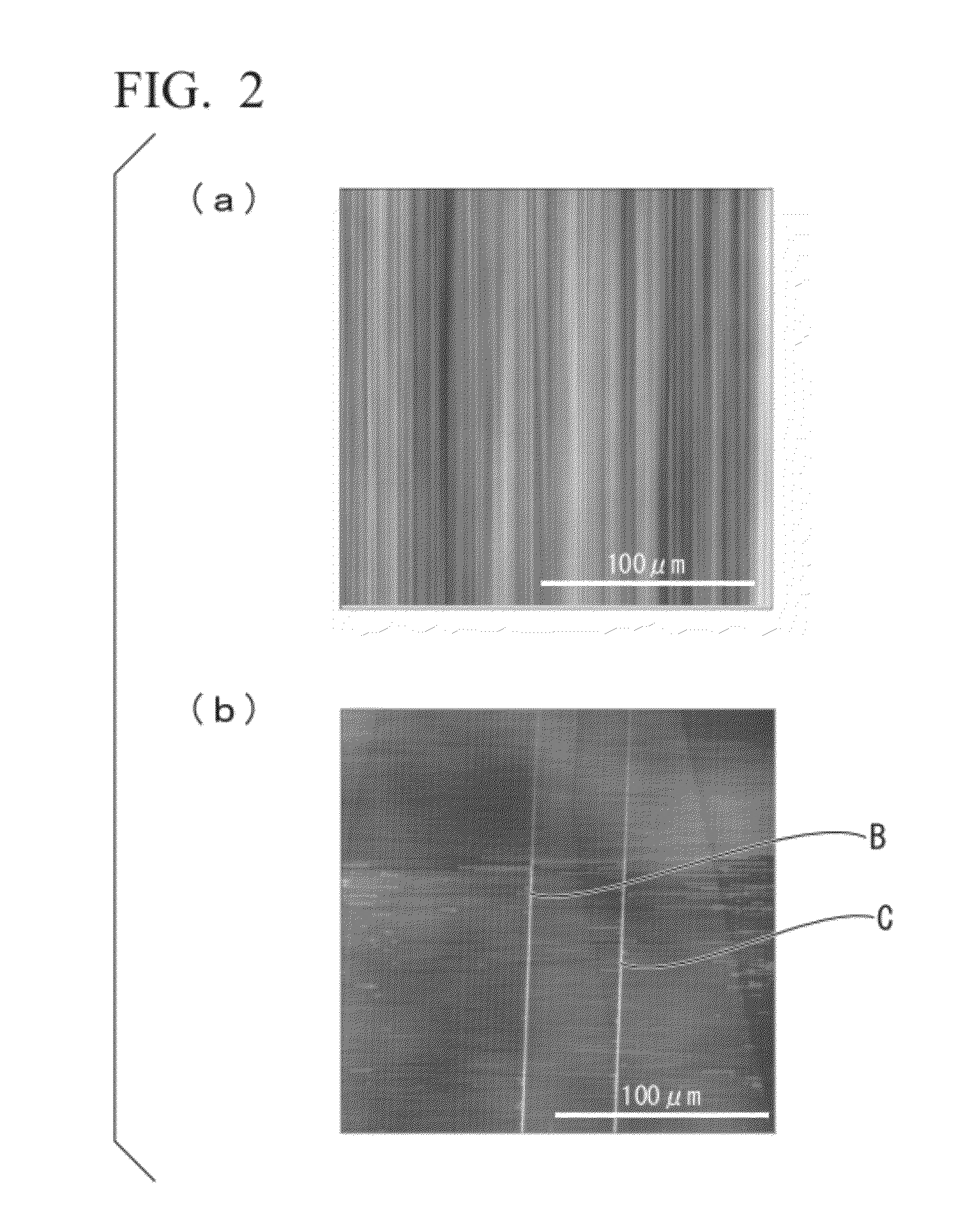
[0123]The cleaning (gas etching) process was performed for 10 minutes with the flow rate of a hydrogen gas of 90 slm, the reactor pressure of 200 mbar, and substrate temperature o...

embodiment 2

[0126]The SiC epitaxial wafer was manufactured under the same condition as Embodiment 1 except for the gas etching condition. Embodiment 2 is different from Embodiment 1 from the viewpoint that the gas etching process is performed through addition of SiH4 gas having the concentration of 0.008 mol % to the hydrogen gas.

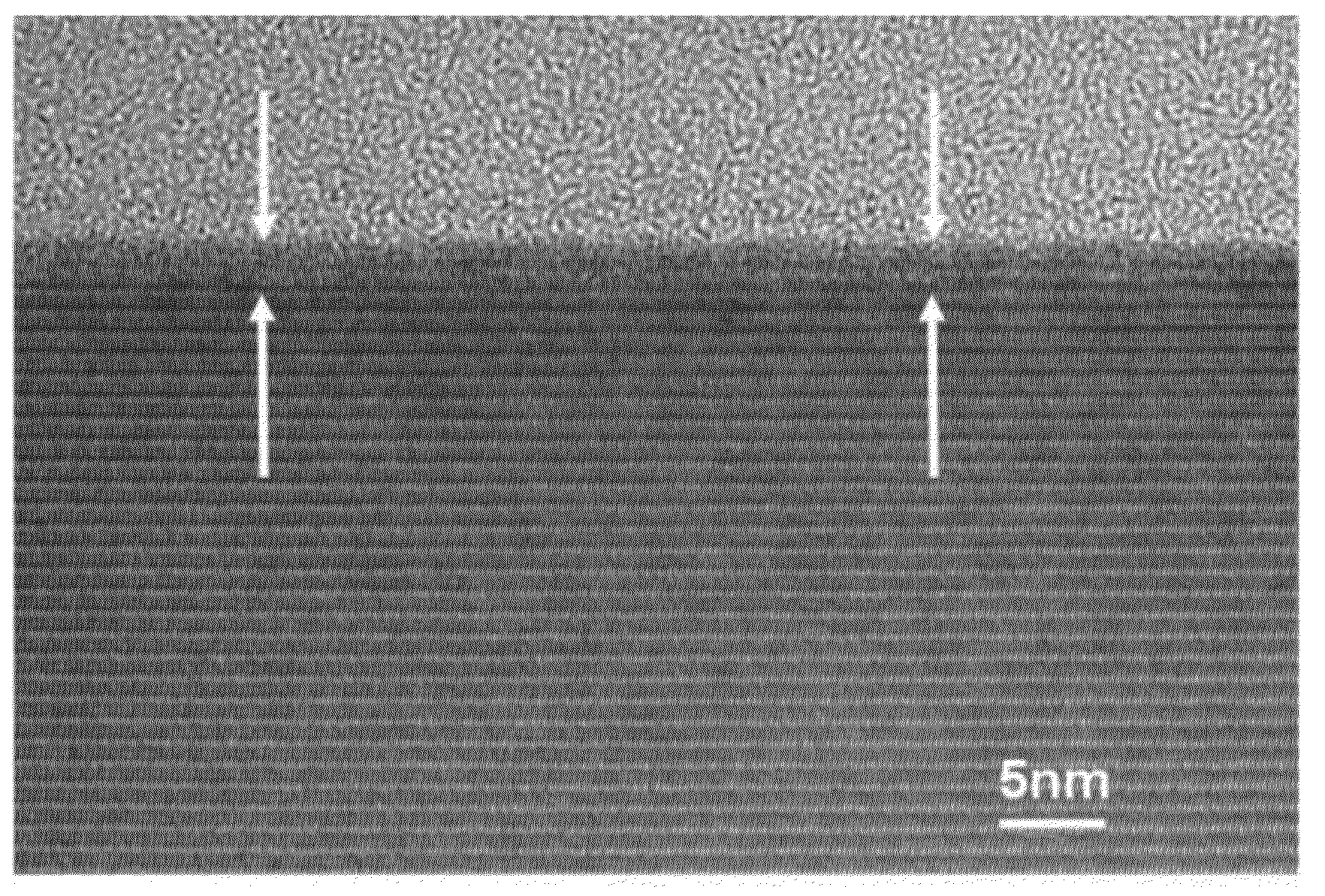
[0127]The SiC epitaxial wafer as described above was measured through the optical surface inspection device and the extensive observation type AFM. In the same manner as Embodiment 1, an image was observed. Rq measured by the optical surface inspection device was 1.1 nm, Rq measured by the extensive observation type AFM was 0.4 nm, and the maximum height difference Ry was 0.7 nm.


PUM


Abstract

Provided is a silicon carbide epitaxial wafer, the entire surface of which is free of step bunching. Also provided is a method for manufacturing said silicon carbide epitaxial wafer. The provided method for manufacturing a silicon carbide semiconductor device includes: a step wherein a 4H—SiC single-crystal substrate having an off-axis angle of 5° or less is polished until the lattice disorder layer on the surface of the substrate is 3 nm or less; a step wherein, in a hydrogen atmosphere, the polished substrate is brought to a temperature between 1400° C. and 1600° C. and the surface of the substrate is cleaned; a step wherein silicon carbide is epitaxially grown on the surface of the cleaned substrate as the amounts of SiH4 gas and C3H8 gas considered necessary for epitaxially growing silicon carbide are supplied simultaneously at a carbon-to-silicon concentration ratio between 0.7 and 1.2 to 1; and a step wherein the supply of SiH4 gas and the supply of C3H8 gas are cut off simultaneously, the substrate temperature is maintained until the SiH4 gas and the C3H8 gas are evacuated, and then the temperature is decreased.

Description

TECHNICAL FIELD[0001]The present invention relates to a silicon carbide epitaxial wafer and a manufacturing method therefor, and more particularly to a silicon carbide (SiC) epitaxial wafer that is free of step bunching, and a manufacturing method therefor.[0002]Priority is claimed on Japanese Patent Application No. 2009-198872 filed in the Japan Patent Office on Aug. 28, 2009, the contents of which are incorporated herein by reference.BACKGROUND ART[0003]In response to the problem of global warming, improvements in energy-saving technology have been demanded. Amongst many technical fields, power electronics technology to reduce energy loss during power conversion is of great importance. Although improvements to power electronics have been made regarding the technical performance using related art silicon (Si) semiconductors, performance improvement has reached a limit due to limitations of the material properties of silicon. Therefore, a silicon carbide (SiC) having a greater physi...

Claims


Application Information

Patent Timeline
IPC IPC(8): H01L29/161H01L21/20
CPCC30B25/20C30B29/36H01L21/02378H01L21/02433H01L29/1608H01L21/02587H01L21/0262H01L21/02658H01L29/0684H01L21/02529H01L21/20
Inventor MOMOSE, KENJITAJIMA, YUTAKASAKAGUCHI, YASUYUKIODAWARA, MICHIYAMIYASAKA, YOSHIHIKO
Owner RESONAC CORP
Why Eureka
Try Eureka