Diffusion barrier structure, transparent conductive structure and method for making the same

a technology of diffusion barrier and transparent conductive, which is applied in the direction of vacuum evaporation coating, transportation and packaging, synthetic resin layered products, etc., can solve the problems of increasing the cost of complex signal processing electronics, and achieve the effect of increasing the crystallinity of ito film and reducing the resistance value of ito film

Inactive Publication Date: 2012-06-21
INNOVATION & INFINITY GLOBAL
View PDF2 Cites 31 Cited by
  • Summary
  • Abstract
  • Description
  • Claims
  • Application Information

AI Technical Summary

Benefits of technology

[0012]In conclusion, because the first oxide layers (such as SiO2) and the second oxide layers (such as Al(Li)Ox) are stacked on top of each other alternately, the diffusion barrier structure can not only avoid generating the interreaction and interdiffusion between every two layers of the transparent conductive structure, but also reduce the influence of oxygen, water vapor, other chemical substances on the transparent conductive film such as ITO conductive layer. Hence, when an ITO film is formed on the transparent conductive film by sputtering, the crystallinity of the ITO film is increased and the resistance value of the ITO film is decreased.

Problems solved by technology

Capacitive touch screens are not affected by outside elements and have high clarity, but their complex signal processing electronics increase their cost.

Method used


Image

  • Diffusion barrier structure, transparent conductive structure and method for making the same
  • Diffusion barrier structure, transparent conductive structure and method for making the same
  • Diffusion barrier structure, transparent conductive structure and method for making the same

Examples


first embodiment

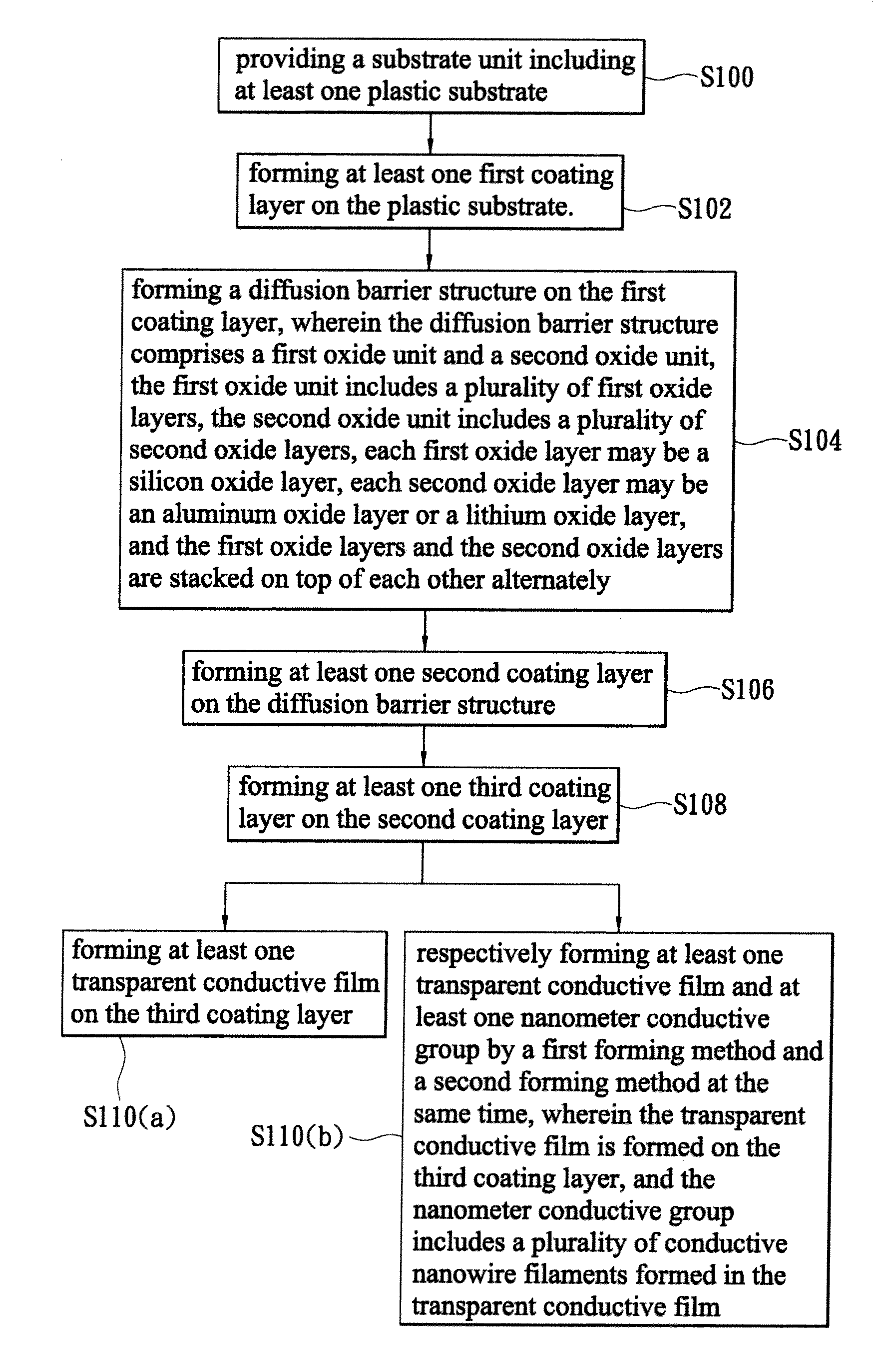
[0018]Referring to FIGS. 1A, 1B and 1C, the instant disclosure a method for making a transparent conductive structure Z. The method comprises some steps from S100 to S110(a), as follows:

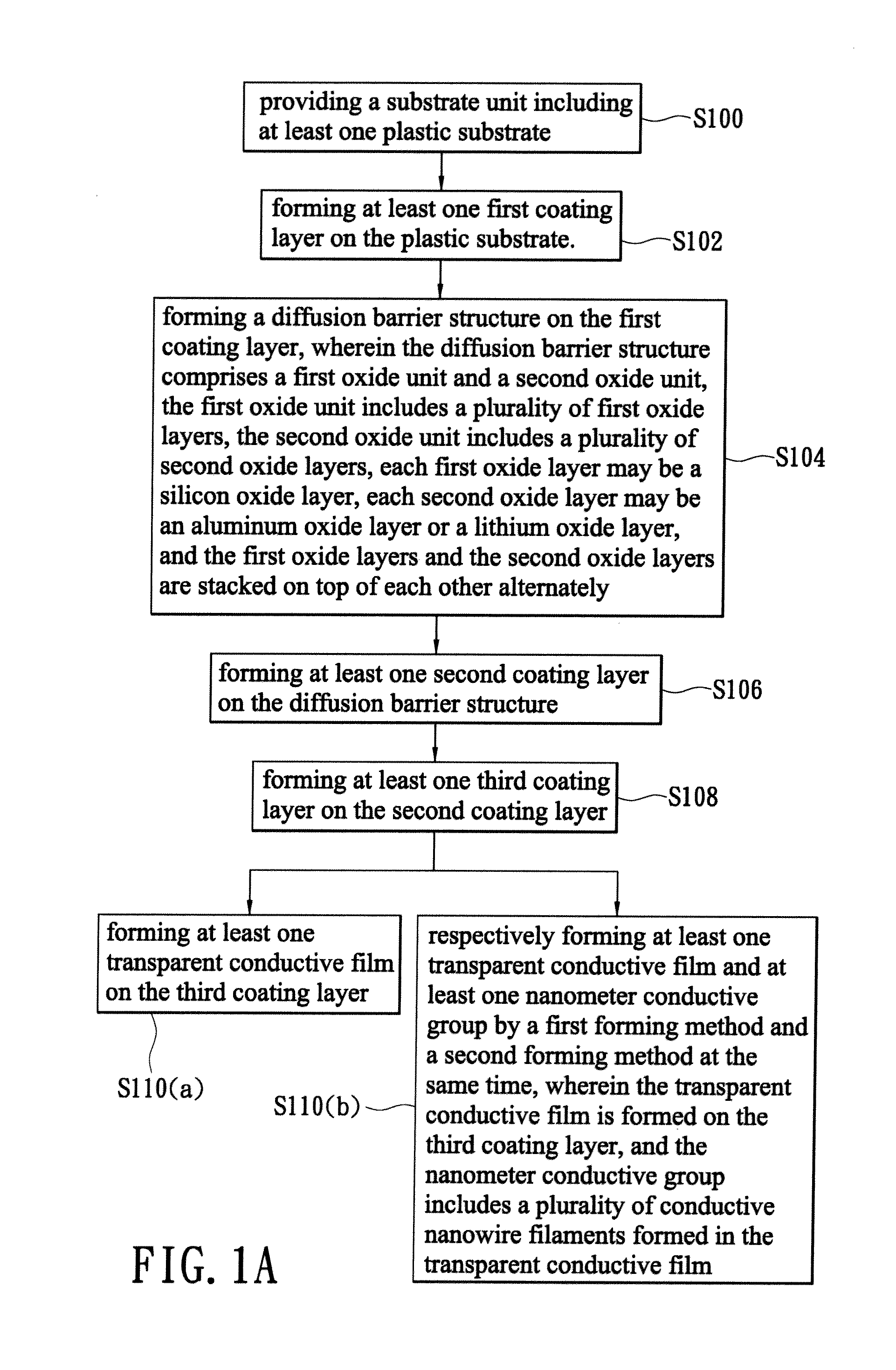
[0019]The step S100 is that: first, referring to FIGS. 1A and 1B, providing a substrate unit 1 including at least one plastic substrate 10. For example, the plastic substrate 10 may be made of PET (polyethylene Terephthalate), PC (Poly Carbonate), PE (polyethylene), PVC (Poly Vinyl Chloride), PP (Poly Propylene), PS (Poly Styrene) or PMMA (Polymethylmethacrylate) according to different requirements.

[0020]The step S102 is that: referring to FIGS. 1A and 1B, forming at least one first coating layer 20 on the plastic substrate 10. For example, the first coating layer 20 may be a ultraviolet (UV) curing layer, and the first coating layer 20 has a thickness of between about 6 μm and 10 μm according to different requirements.

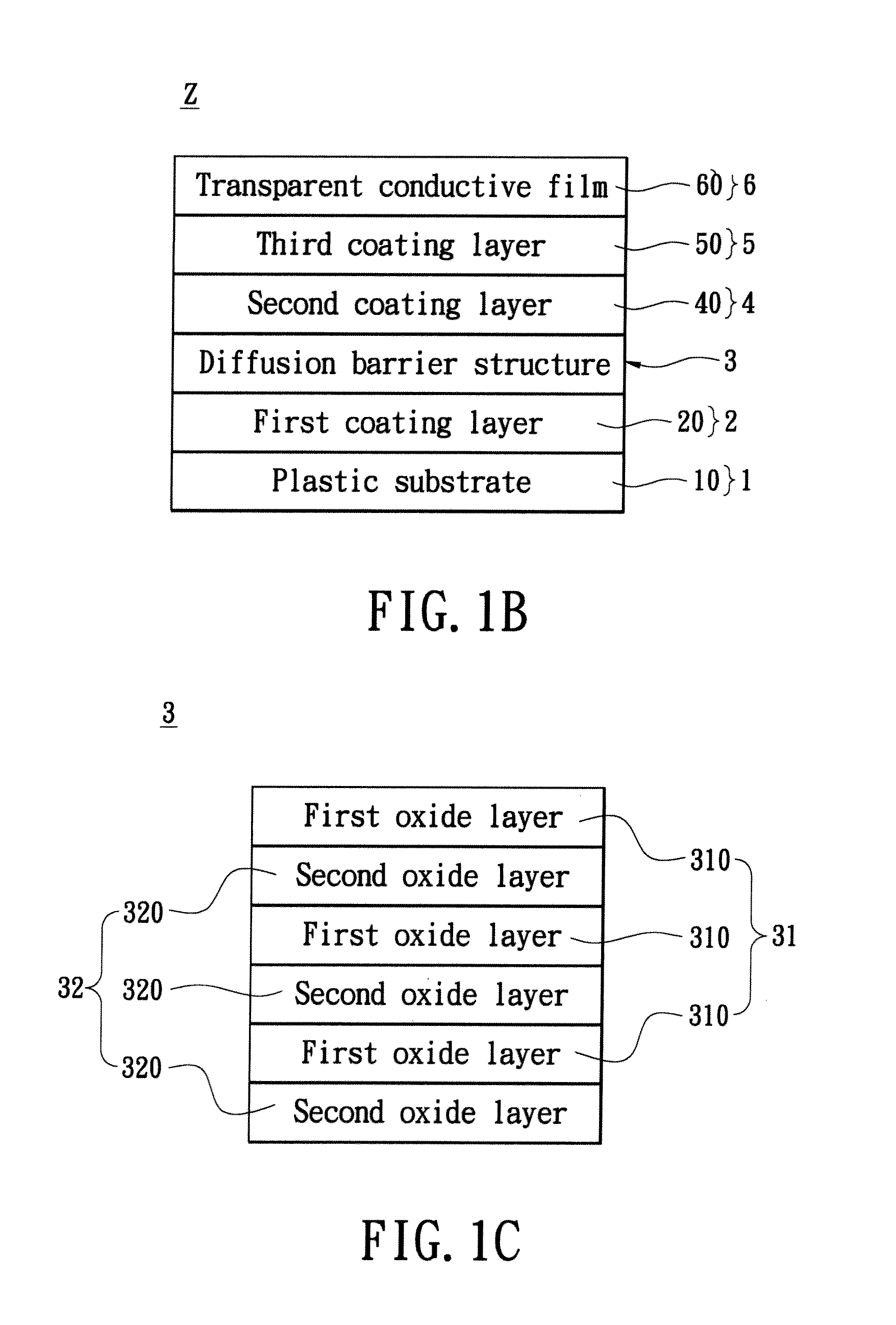
[0021]The step S104 is that: referring to FIGS. 1A, 1B and 1C, forming a diffusion...

second embodiment

[0028]Moreover, the instant disclosure a method for making a transparent conductive structure Z as shown in FIG. 1A. The method comprises some steps from S100 to S110(b), where the step S110(b) is that: respectively forming at least one transparent conductive film 60 and at least one nanometer conductive group 61 by a first forming method and a second forming method at the same time (it means both the transparent conductive film 60 and the nanometer conductive group 61 are formed simultaneously), wherein the transparent conductive film 60 is formed on the third coating layer 50, and the nanometer conductive group 61 includes a plurality of conductive nanowire filaments 610 formed in the transparent conductive film 60 (as shown in FIG. 2).

[0029]Hence, in the step S110(b) of the second embodiment, the first forming method may be sputter deposition and the second forming method may be vapor deposition, thus the transparent conductive film 60 and the nanometer conductive group 61 can be...


PUM

PropertyMeasurementUnit
thicknessaaaaaaaaaa
thicknessaaaaaaaaaa
thicknessaaaaaaaaaa

Abstract

A transparent conductive structure includes a substrate unit, a first coating unit, a diffusion barrier structure, a second coating unit, a third coating unit and a conductive unit. The substrate unit includes a plastic substrate. The first coating unit includes a first coating layer formed on the plastic substrate. The diffusion barrier structure is formed on the first coating layer. The diffusion barrier structure includes a first oxide unit having a plurality of first oxide layers and a second oxide unit having a plurality of second oxide layers. The first oxide layers and the second oxide layers are stacked on top of each other alternately. The second coating unit includes a second coating layer formed on the diffusion barrier structure. The third coating unit includes a third coating layer formed on the second coating layer. The conductive unit includes a transparent conductive film formed on the third coating layer.

Description

BACKGROUND OF THE INVENTION[0001]1. Field of the Invention[0002]The instant disclosure relates to a diffusion barrier structure, a transparent conductive structure and a method for making the same, and more particularly, to a diffusion barrier structure, a transparent conductive structure and a method for making the same applied to a touch panel.[0003]2. Description of Related Art[0004]In 1970, touch panel is originated for military usage in United States of America. Until 1980, technologies related to touch panel were published and utilized to be other applications. Now, touch panel is universal and applied to replace input device like keyboard or mouse. Especially, most of electrical equipments such as Automatic Teller Machine (ATM), Kiosks, Point of Service (POS), household appliances, industrial electronics and so on are equipped with touch panel and its technologies to make input easily. In addition, more and more the consumer products take this trend to make them thin, light, ...

Claims


Application Information

Patent Timeline
Patent Type & Authority Applications(United States)
IPC IPC(8): B32B7/02C23C16/40B32B9/00C23C14/34B82Y30/00
CPCY10T428/24975B82Y30/00Y10T428/249924Y10T428/31507
Inventor CHU, CHAO-CHIEH
Owner INNOVATION & INFINITY GLOBAL
Why Eureka
Try Eureka