

Label having an electronic functional element
- Summary
- Abstract
- Description
- Claims
- Application Information
AI Technical Summary
Benefits of technology
Problems solved by technology
Method used
Image

Examples
Embodiment Construction
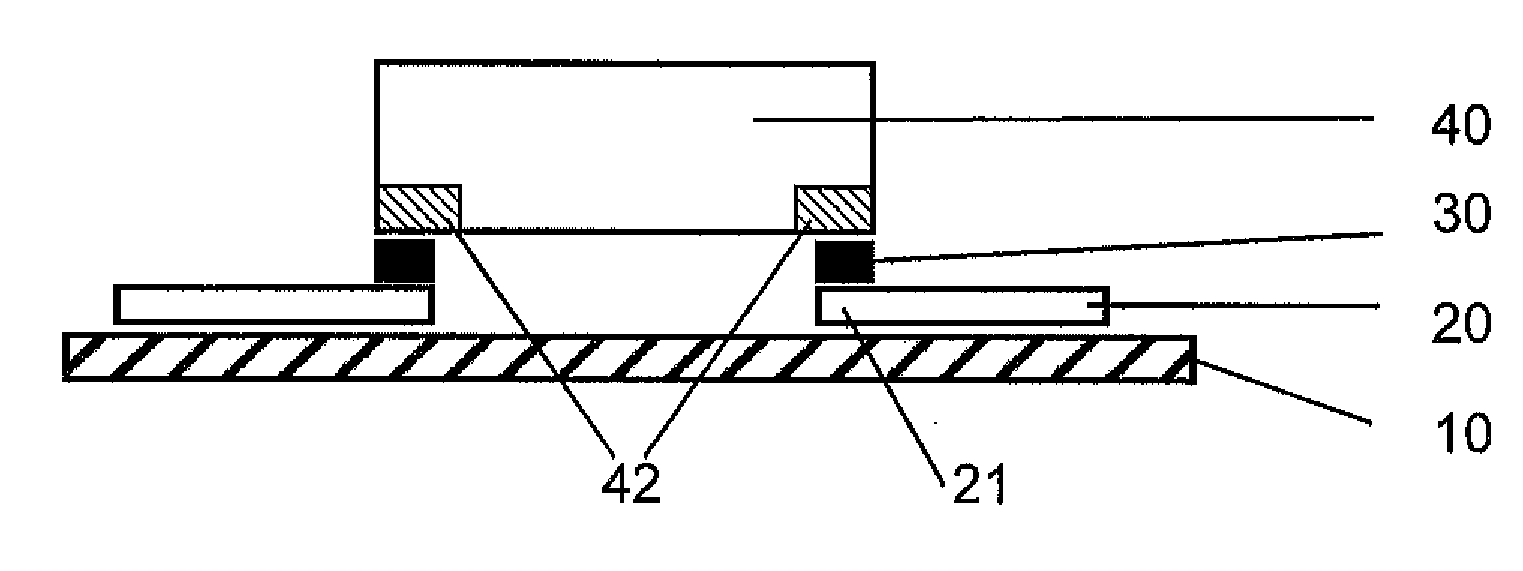
[0033]The following description explains the electronic functional label, as well as its production and use. In this connection, the ideas according to the invention are not restricted to the exemplary embodiments described. Further embodiments that form the basis of the fundamental principle of this invention are also possible.
[0034]FIG. 1 shows a first embodiment of a film structure 1 according to the invention. First, electrically conductive structures 20 are applied to a film substrate 10. Preferably, these electrically conductive structures 20 are produced by application of an electrically conductive lacquer, using a printing process. For example, silver conductive paste, carbon black, an organic conductive paste, or another substance having conductive particles can be used as an electrically conductive lacquer.
[0035]Alternative methods for applying electrically conductive structures to carrier substrate 10 are also possible, however. For example, a copper foil, an ITO coating,...
PUM
| Property | Measurement | Unit |
|---|---|---|
| Temperature | aaaaa | aaaaa |
| Thickness | aaaaa | aaaaa |
| Electrical conductivity | aaaaa | aaaaa |
Abstract
Description
Claims
Application Information