Diode structures with controlled injection efficiency for fast switching

a diode and efficiency control technology, applied in the direction of semiconductor devices, electrical apparatus, transistors, etc., can solve the problems of high modulation, slow switching speed of diodes, and high power consumption of pin diodes formed with conventional structures, so as to reduce minority charges, soft switching, and low injection efficiency

Active Publication Date: 2012-08-02
ALPHA & OMEGA SEMICON INC
View PDF8 Cites 54 Cited by
  • Summary
  • Abstract
  • Description
  • Claims
  • Application Information

AI Technical Summary

Benefits of technology

[0010]It is therefore an aspect of the present invention to provide a new and improved device configuration of PiN diodes with an added buffer region to lower the injection efficiency to lower minority charges in the drift region and to tailor its profile to achieve soft switching. In addition, the device requires minimal or no conventional lifetime control techniques, which makes its characteristics stable at high temperature.

Problems solved by technology

PiN diodes formed with conventional structures are still limited by a high modulation due to limited options for controlling the amount of anode and cathode electric charges injected as carriers into the intrinsic (or lowly doped) semiconductor layer typically disposed between the more heavily doped N-type and P-type layers.
The difficulties cause the diode device to have a slow switching speed.
Furthermore, the limited control of the charges also causes high reverse current and recovery time, which results in higher power consumptions and low operation efficiency.
But these techniques require extra processing steps that add to the cost, and also cause increased leakage at high cathode biases.
Furthermore, changes on the lifetime with temperature cause the diode reverse recovery to degrade significantly at high temperatures for lifetime controlled devices.
This high voltage PiN diode has a problem of high modulation which causes high switching losses and low switching speeds.
The high modulation means high carrier injection and high stored charges.
This improves the forward conductivity of the diode, but leads to high switching losses and slow switching speed because those stored charges need to removed from the lightly doped layer 2 when the diode turns off.
However, the lowering of topside P doping concentration is limited by punch through constraints.
There needs to be enough P charge present to bring the electric field down to zero or else the device will punch through and leak heavily.
Thus despite these steps, there are still limitations in the improvement of the device switching speed.

Method used


Image

  • Diode structures with controlled injection efficiency for fast switching
  • Diode structures with controlled injection efficiency for fast switching
  • Diode structures with controlled injection efficiency for fast switching

Examples


Embodiment Construction

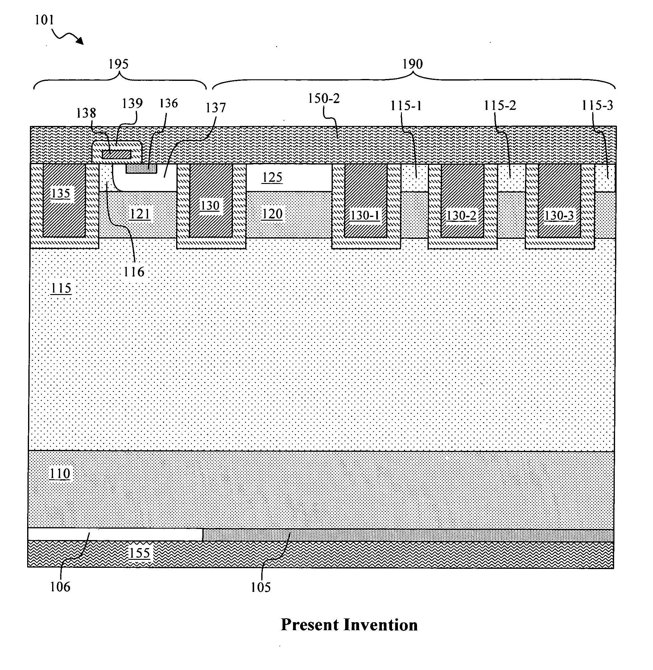
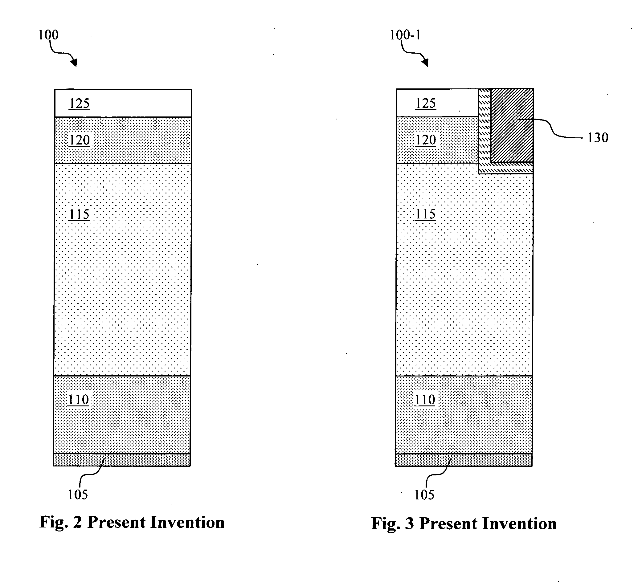
[0035]Referring to FIG. 2 for a cross sectional view of a PiN diode 100 of this invention. The PiN diode 100 has a heavily doped N type bottom layer 105. By way of example, the PiN diode 100 may initially be supported on a thick N-type bottom substrate layer with a backside grinding process carried out to remove a bottom portion or all of the bottom substrate layer followed by a backside implanting and anneal process to form a thin layer of heavily doped N-doped bottom layer 105. Typical charge concentration in this region may be about 5E12 / cm2. The bottom heavily N doped layer 105 supports a less heavily doped N buffer layer 110 for soft recovery with typical doping and thickness of about 5E14 / cm3 and 15 um respectively. Above that N buffer layer 110 is the lightly doped N layer 115 (e.g. an epitaxial layer) with typical doping in the range of 2E13-1E14 / cm3 and thickness of 30-90 um, depending on the breakdown voltage. The PiN diode 100 further includes a heavily doped N-type buffe...


PUM


Abstract

This invention discloses a semiconductor device disposed in a semiconductor substrate. The semiconductor device includes a first semiconductor layer of a first conductivity type on a first major surface. The semiconductor device further includes a second semiconductor layer of a second conductivity type on a second major surface opposite the first major surface. The semiconductor device further includes an injection efficiency controlling buffer layer of a first conductivity type disposed immediately below the second semiconductor layer to control the injection efficiency of the second semiconductor layer.

Description

BACKGROUND OF THE INVENTION[0001]1. Field of the Invention[0002]The invention relates generally to the configurations and methods of manufacturing semiconductor power devices. More particularly, this invention relates to a device configuration and method of manufacturing a high voltage PiN (P-type / intrinsic / N-type) diode with low injection efficiency for improving the switching speed.[0003]2. Description of the Prior Art[0004]PiN diodes formed with conventional structures are still limited by a high modulation due to limited options for controlling the amount of anode and cathode electric charges injected as carriers into the intrinsic (or lowly doped) semiconductor layer typically disposed between the more heavily doped N-type and P-type layers. The difficulties cause the diode device to have a slow switching speed. Furthermore, the limited control of the charges also causes high reverse current and recovery time, which results in higher power consumptions and low operation efficie...

Claims


Application Information

Patent Timeline
Patent Type & Authority Applications(United States)
IPC IPC(8): H01L29/72H01L21/331
CPCH01L29/7391
Inventor BOBDE, MADHURNAIK, HARSHGUAN, LINGPENGBHALLA, ANUPLUI, SIK
Owner ALPHA & OMEGA SEMICON INC
Why Eureka
Try Eureka