

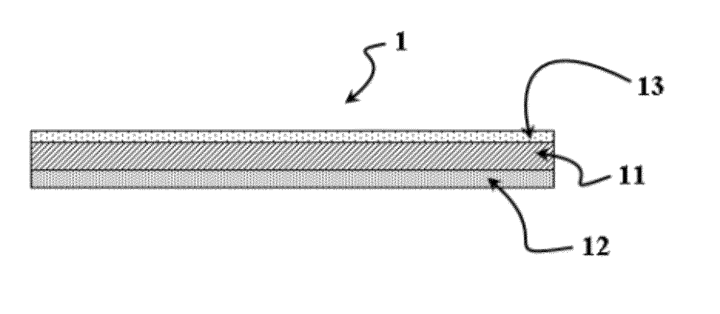
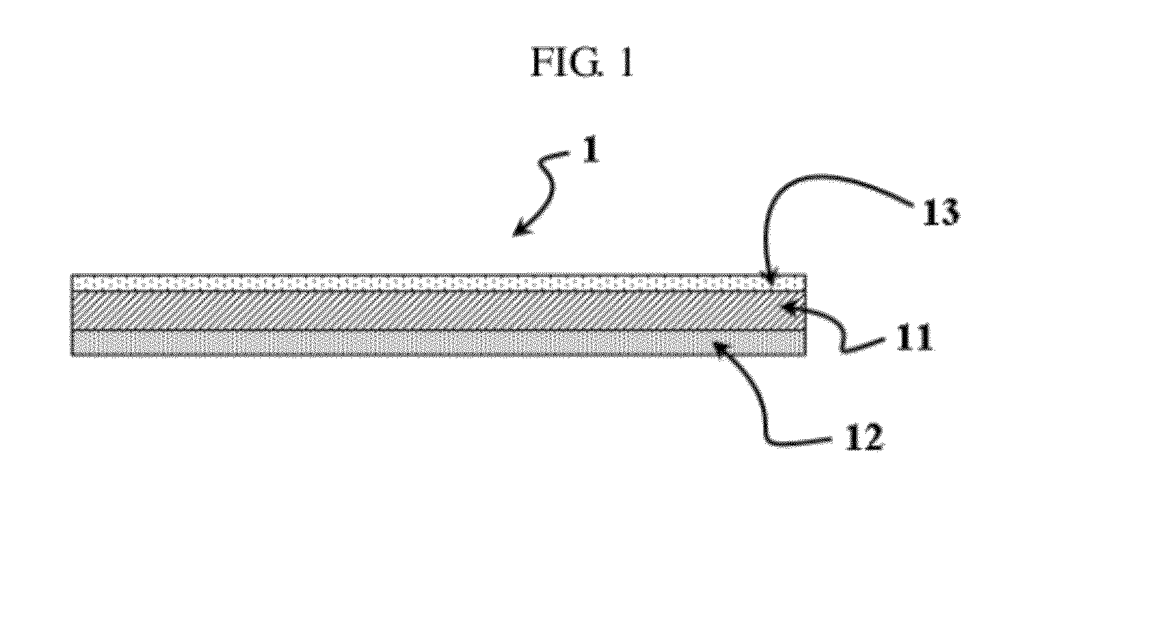
Wafer processing sheet
a wafer and processing sheet technology, applied in the field of wafer processing sheet, can solve the problems of reducing relaxation, reducing the protection of the wafer, and increasing the probability of damage to the wafer, so as to effectively protect the wafer during the wafer processing, and increase the cross-linking density. the effect of high density
- Summary
- Abstract
- Description
- Claims
- Application Information
AI Technical Summary
Benefits of technology
Problems solved by technology
Method used
Image

Examples
example 1
[0079]Formation of Anti-Blocking Layer
[0080]A monomer mixture of 90 parts by weight of methyl methacrylate (MMA) and 10 parts by weight of hydroxyethyl methacrylate (HEMA) was polymerized to prepare an acrylic polymer having a solid content of 20 wt %. Subsequently, relative to 100 parts by weight of the acrylic polymer as prepared above, 10 parts by weight of an isocyanate curing agent (TDI) was mixed therewith to prepare a coating solution. Then, the coating solution as prepared above was coated on a polyester releasing film using a bar coater to have a thickness of 2 μm after being dried; drying and aging of the coated layer was performed under the appropriate conditions so as to form an anti-blocking layer.
[0081]Formation of Substrate
[0082]A monomer mixture including 70 parts by weight of 2-ethylhexyl acrylate (2-EHA), 27 parts by weight of isobornyl acrylate (IBOA) and 3 parts by weight of hydroxyethyl acrylate (2-HEA) was input into a 1 L reactor containing refluxed nitrogen g...
example 2
[0085]A sheet for processing a wafer was formed according to the same method as described in Example 1, except that, when the anti-blocking layer was formed, the isocyanate curing agent (TDI) was not used, such that an anti-blocking layer including uncured acrylic polymer was formed.
example 3
[0086]A sheet for processing a wafer was formed according to the same method as described in Example 1, except that, when an anti-blocking layer was formed, cellulose acetate resin was used instead of the mixture including acrylic polymer and the isocyanate curing agent, such that an anti-blocking layer including uncured cellulose acetate resin was formed.
PUM
| Property | Measurement | Unit |
|---|---|---|
| Temperature | aaaaa | aaaaa |
| Thickness | aaaaa | aaaaa |
| Thickness | aaaaa | aaaaa |
Abstract
Description
Claims
Application Information