Light-Emitting Element, Light-Emitting Device, and Display Device

a technology of light-emitting devices and light-emitting elements, which is applied in the direction of organic semiconductor devices, semiconductor devices, semiconductor/solid-state device details, etc., can solve the problems of difficult to increase yield or productivity, and achieve high productivity, low power consumption, and high color purity

Active Publication Date: 2012-08-16
SEMICON ENERGY LAB CO LTD
View PDF6 Cites 69 Cited by
  • Summary
  • Abstract
  • Description
  • Claims
  • Application Information

AI Technical Summary

Benefits of technology

[0019]According to one embodiment of the present invention, a display device can be manufactured with high productivity.
[0020]Further, according to one embodiment of the present invention, a high-definition display device with high color purity can be provided.
[0021]Further, according to one embodiment of the present invention, a display device with low power consumption can be provided.

Problems solved by technology

A method in which selective deposition of light-emitting materials is performed for each pixel has a complicated process; thus, yield or productivity is difficult to increase.

Method used


Image

  • Light-Emitting Element, Light-Emitting Device, and Display Device
  • Light-Emitting Element, Light-Emitting Device, and Display Device
  • Light-Emitting Element, Light-Emitting Device, and Display Device

Examples


embodiment 1

[0030]In this embodiment, one embodiment of an EL display device will be described with reference to FIGS. 1A and 1B, FIG. 2, and FIGS. 3A to 3C.

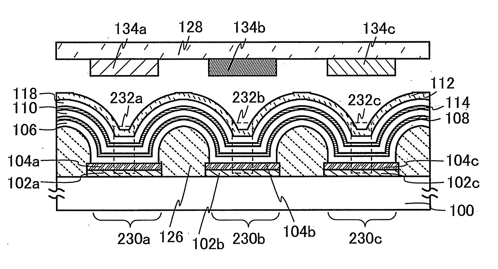
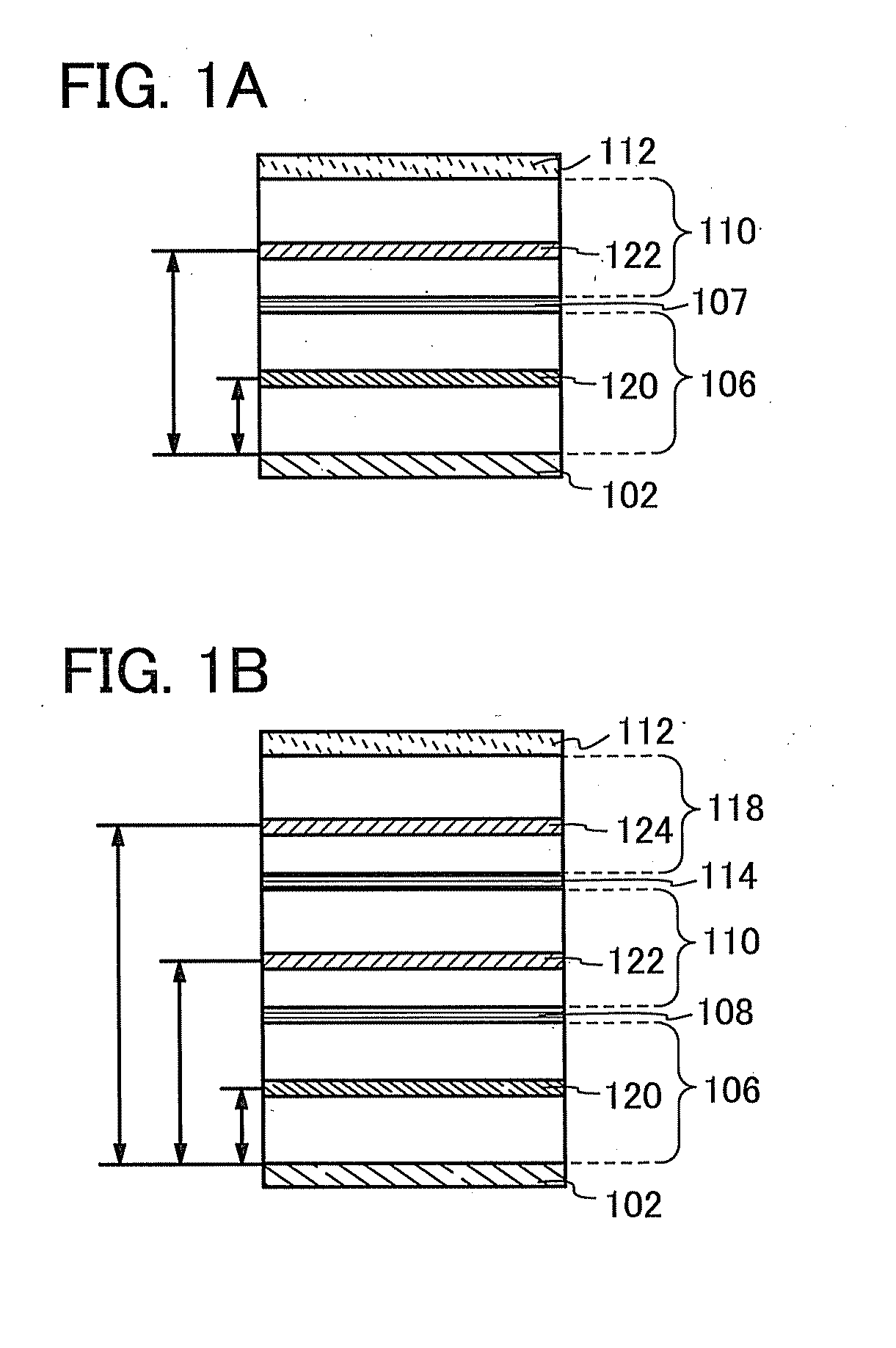
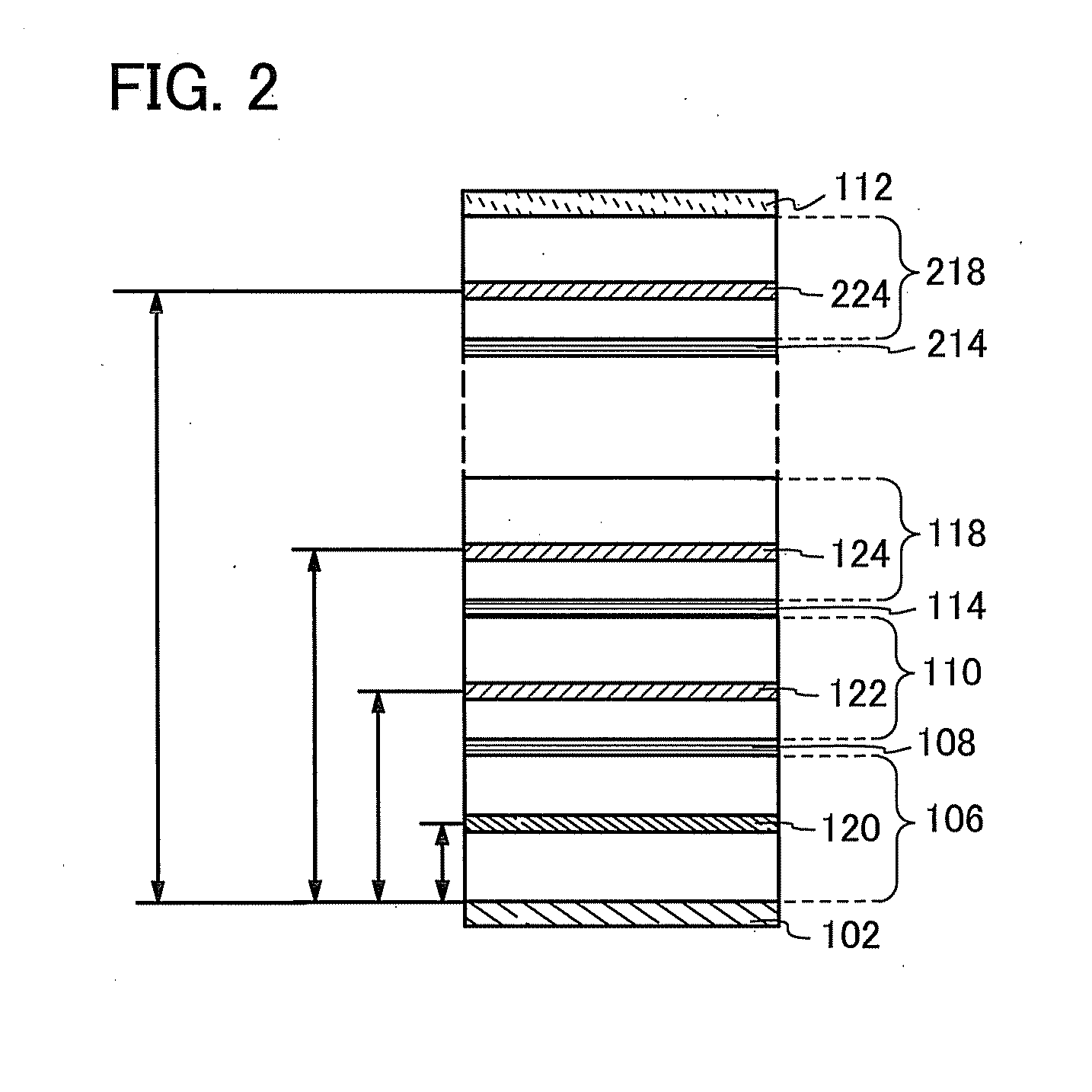
[0031]FIG. 1A illustrates a structure of a light-emitting element according to this embodiment. The light-emitting element illustrated in FIG. 1A includes an electrode 102 having a reflective property, and a first EL layer 106, a charge generation layer 107, a second EL layer 110, and an electrode 112 having a light-transmitting property which are stacked in this order over the electrode 102 having a reflective property. Light emitted from the light-emitting element is emitted from the electrode 112 side.

[0032]In FIG. 1A, the first EL layer 106 includes at least a first light-emitting layer 120. The second EL layer 110 includes at least a second light-emitting layer 122. Note that each of the first EL layer 106 and the second EL layer 110 can have a stacked-layer structure including functional layers such as a hole-injection layer, a hole-t...

embodiment 2

[0141]In this embodiment, an active matrix display device that is one embodiment of the present invention will be described with reference to FIGS. 4A and 4B. FIG. 4A is a plan view illustrating a display device. FIG. 4B is a cross-sectional view taken along line A-B and C-D in FIG. 4A.

[0142]In the display device illustrated in FIGS. 4A and 4B, an element substrate 410 and a sealing substrate 404 are attached to each other with a sealant 405, and a driver circuit portion (a source-side driver circuit 401 and a gate side driver circuit 403) and a pixel portion 402 including a plurality of pixels are provided.

[0143]Note that a wiring 408 is a wiring for transmitting signals that are to be inputted to the source side driver circuit 401 and the gate side driver circuit 403, and receives a video signal, a clock signal, a start signal, a reset signal, and the like from a flexible printed circuit (FPC) 409 which serves as an external input terminal. Although only the FPC is illustrated her...

embodiment 3

[0180]A display device disclosed in this specification can be applied to a variety of electronic appliances (including game machines). Examples of electronic devices include a television set (also referred to as a television or a television receiver), a monitor of a computer or the like, a camera such as a digital camera or a digital video camera, a digital photo frame, a mobile phone handset (also referred to as a mobile phone or a mobile phone device), a portable game console, a portable information terminal, an audio reproducing device, and a large-sized game machine such as a pachinko machine.

[0181]FIG. 5A illustrates a laptop personal computer, which includes a main body 3001, a housing 3002, a display portion 3003, a keyboard 3004, and the like. By applying the display device described in Embodiment 1 or 2 to the display portion 3003, the laptop personal computer can have a high level of definition and consumes a small amount of power.

[0182]FIG. 5B illustrates a personal digit...


PUM


Abstract

A light-emitting element with which a reduction in power consumption and an improvement in productivity of a display device can be achieved is provided. A technique of manufacturing a display device with high productivity is provided. The light-emitting element includes an electrode having a reflective property, and a first light-emitting layer, a charge generation layer, a second light-emitting layer, and an electrode having a light-transmitting property stacked in this order over the electrode having a reflective property. The optical path length between the electrode having a reflective property and the first light-emitting layer is one-quarter of the peak wavelength of the emission spectrum of the first light-emitting layer. The optical path length between the electrode having a reflective property and the second light-emitting layer is three-quarters of the peak wavelength of the emission spectrum of the second light-emitting layer.

Description

BACKGROUND OF THE INVENTION[0001]1. Field of the Invention[0002]One embodiment of the present invention relates to a light-emitting element exhibiting electroluminescence, a display device including the light-emitting element, and manufacturing methods of the light-emitting element and the display device.[0003]2. Description of the Related Art[0004]In recent years, an electroluminescent (also referred to as EL) display device has attracted attention as a display device with reduced thickness and weight (i.e., so-called flat panel display).[0005]Light-emitting elements using light-emitting materials emitting light of different colors are provided as light-emitting elements used in pixels in an EL display device, so that full-color display can be performed.[0006]For such an EL display device, a method is used in which selective deposition of light-emitting materials in a minute pattern is performed for each pixel by an evaporation method using a metal mask.[0007]However, a shape defec...

Claims


Application Information

Patent Timeline
Patent Type & Authority Applications(United States)
IPC IPC(8): H01L33/08H01L33/60H01L27/15
CPCH01L51/5044H01L2251/5376H01L51/5278H01L51/5265H10K59/32H10K50/131H10K50/852H10K50/19H10K2101/27H01L23/145H10K59/38H10K50/13H10K50/818H10K50/828H10K50/856
Inventor SEO, SATOSHISASAKI, TOSHIKIOHSAWA, NOBUHARUUSHIKUBO, TAKAHIROYAMAZAKI, SHUNPEI
Owner SEMICON ENERGY LAB CO LTD
Why Eureka
Try Eureka