Memory circuit, memory unit, and signal processing circuit

a memory circuit and signal processing technology, applied in the field of memory, can solve the problems of reducing the operation speed of the memory circuit, affecting the data return speed of the external memory unit, and affecting the data return speed of the volatile memory unit, so as to increase reduce the number of possible data rewriting operations, and reduce the mobility

Inactive Publication Date: 2012-10-04
SEMICON ENERGY LAB CO LTD
View PDF7 Cites 30 Cited by
  • Summary
  • Abstract
  • Description
  • Claims
  • Application Information

AI Technical Summary

Benefits of technology

[0038]While a supply voltage is supplied to the memory circuit and the clock signal and the inverted signal of the clock signal whose levels (potentials) periodically change between high and low levels are input, the memory circuit holds input data in the feedback loop, and outputs the data held in the feedback loop. Here, a transistor having a low mobility, e.g., a transistor whose channel is formed in an oxide semiconductor layer is not present in the feedback loop. Thus, the feedback loop achieves high-speed data writing and reading, increasing the data writing and reading speed (operation speed) of the memory circuit.
[0039]The memory circuit can hold stored content (data) for a long period of time even while the supply of the supply voltage is stopped. Therefore, the fatigue of the memory circuit 100 due to the repetition of data rewriting can be made insignificant, increasing the number of possible data rewriting operations.
[0040]In addition, a path for writing data held in the feedback loop into the capacitor (data saving path) and a path for returning the data held in the capacitor to the feedback loop (data returning path) are separate. Here, a transistor whose off-state current is extremely low needs ...

Problems solved by technology

A memory circuit using a ferroelectric element has a limited number of rewriting operations because it poses a problem, for example, of write error due to ferroelectric material fatigue caused after the repetition of data writing.
This causes a problem, for example, of significant degradation of each memory circuit due to the repetition of data rewriting.
With a method in which data in the vo...

Method used


Image

  • Memory circuit, memory unit, and signal processing circuit
  • Memory circuit, memory unit, and signal processing circuit
  • Memory circuit, memory unit, and signal processing circuit

Examples


embodiment 1

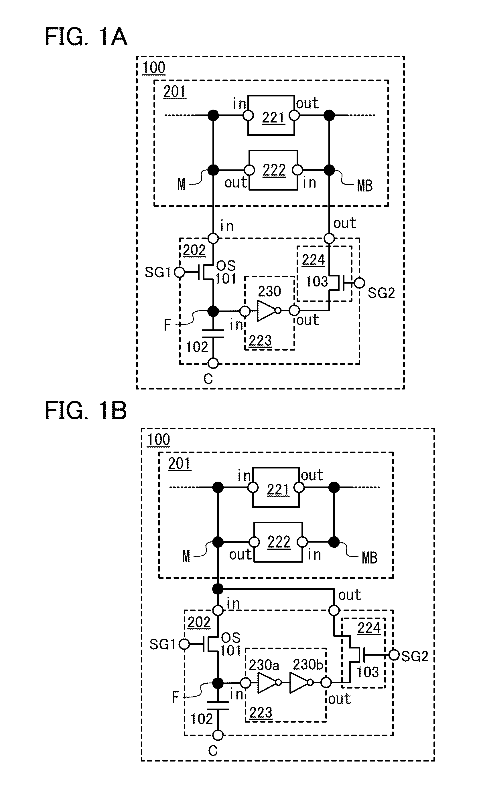
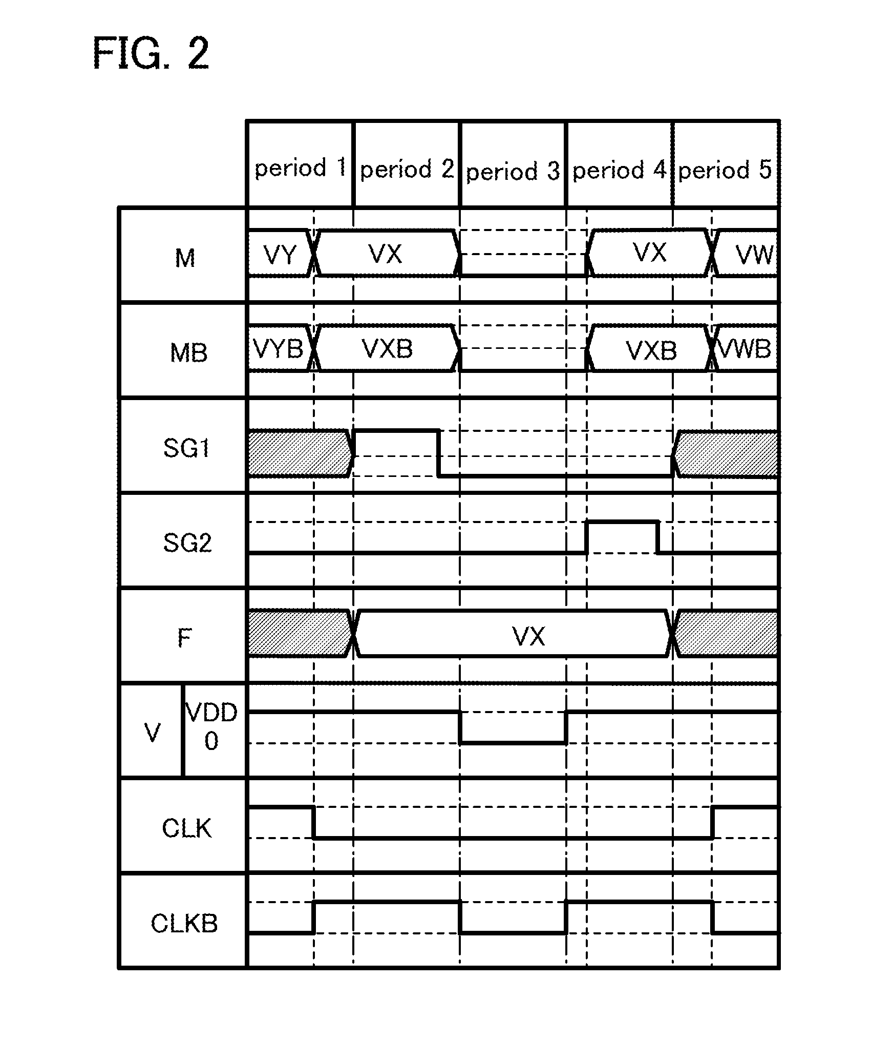
[0060]The following describes one embodiment of a memory circuit according to the present invention. FIG. 1A shows the structure of a memory circuit.

[0061]In FIG. 1A, a memory circuit 100 includes a transistor 101 whose off-state current is extremely low, a capacitor 102, an arithmetic circuit 221, an arithmetic circuit 222, an arithmetic circuit 223, and a switch 224. The transistor 101 is a transistor whose channel is formed in an oxide semiconductor layer as an example, and is represented by “OS”. An output terminal of the arithmetic circuit 221 (represented by “out” in the figure) is electrically connected to an input terminal of the arithmetic circuit 222 (represented by “in” in the figure). The input terminal of the arithmetic circuit 222 is electrically connected to an output terminal of the arithmetic circuit 223 (represented by “out” in the figure) via the switch 224. An output terminal of the arithmetic circuit 222 (represented by “out” in the figure) is electrically conne...

embodiment 2

[0093]This embodiment shows another embodiment of the memory circuit according to the present invention. The configuration of the memory circuit 100 is shown in FIG. 3.

[0094]In FIG. 3, the memory circuit 100 includes a flip-flop circuit 201a, a flip-flop circuit 201b, a circuit 202a, and a circuit 202b. An output terminal of the flip-flop circuit 201a (represented by “out” in the figure) is electrically connected to an input terminal of the flip-flop circuit 201b (represented by “in” in the figure). An input terminal of the flip-flop circuit 201a (represented by “in” in the figure) serves as an input terminal D of the memory circuit 100, while an output terminal of the flip-flop circuit 201b (represented by “out” in the figure) serves as an output terminal Q of the memory circuit 100.

[0095]The circuit 202a and the circuit 202b may have the same configuration as that of the circuit 202 shown in FIG. 1A.

[0096]The flip-flop circuit 201a includes an arithmetic circuit 221a and an arithm...

embodiment 3

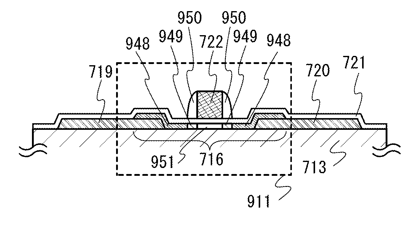
[0119]A method for manufacturing the memory circuit 100 in FIGS. 1A and 1B will be described. This embodiment describes a method for manufacturing the memory circuit 100 referring to elements in the memory circuit 100: the transistor 103, the transistor 101 whose channel is formed in an oxide semiconductor layer, and the capacitor 102. Here, the case where the transistor 103 is a transistor whose channel is formed in a silicon layer is described as an example.

[0120]First, as illustrated in FIG. 5A, an insulating film 701 and a semiconductor film 702 that has been separated from a single crystal semiconductor substrate are formed over a substrate 700.

[0121]Although there is no particular limitation on a material which can be used as the substrate 700, the material needs to have at least heat resistance high enough to withstand the subsequent heat treatment. For example, a glass substrate formed by a fusion process or a float process, a quartz substrate, a semiconductor substrate, a c...


PUM


Abstract

A memory circuit includes a transistor having a channel in an oxide semiconductor layer, a capacitor, a first arithmetic circuit, a second arithmetic circuit, a third arithmetic circuit, and a switch. An output terminal of the first arithmetic circuit is electrically connected to an input terminal of the second arithmetic circuit. The input terminal of the second arithmetic circuit is electrically connected to an output terminal of the third arithmetic circuit via the switch. An output terminal of the second arithmetic circuit is electrically connected to an input terminal of the first arithmetic circuit. An input terminal of the first arithmetic circuit is electrically connected to one of a source and a drain of the transistor. The other of the source and the drain of the transistor is electrically connected to one of a pair of electrodes of the capacitor and to an input terminal of the third arithmetic circuit.

Description

BACKGROUND OF THE INVENTION[0001]1. Field of the Invention[0002]The present invention relates to a memory circuit in which the logic state is not erased after the power is turned off, to a memory unit and a signal processing circuit using the memory circuit, to a method for driving the memory circuit, the memory unit, and the signal processing circuit, and to an electronic device using the signal processing circuit.[0003]2. Description of the Related Art[0004]Signal processing circuits such as central processing units (CPUs) vary in structure depending on the intended use. A signal processing circuit generally has a main memory for storing data or program and other memory units such as a register and a cache memory. A register has a function of temporarily holding data for carrying out arithmetic processing, holding a program execution state, or the like. Meanwhile, a cache memory, which is located between an arithmetic circuit and a main memory, is provided to reduce low-speed acce...

Claims


Application Information

Patent Timeline
IPC IPC(8): G11C11/40
CPCH01L27/1225G11C16/045G11C7/1006H01L27/0688H01L27/06G11C7/10G11C7/22G11C5/14
Inventor KUROKAWA, YOSHIYUKI
Owner SEMICON ENERGY LAB CO LTD
Why Eureka
Try Eureka