Method for fabricating semiconductor device

a semiconductor device and fabrication method technology, applied in the direction of semiconductor devices, electrical devices, transistors, etc., can solve the problems of reducing the total account of the defect semiconductor device, the dimension of the fet and the thickness of the gate oxide, and the increased risk of gate leakage, so as to reduce the total account of the defect semiconductor device, the effect of reducing the etching selectivity and significantly reducing the polymer residue generated in the etching process

Inactive Publication Date: 2012-10-18
UNITED MICROELECTRONICS CORP
View PDF8 Cites 20 Cited by
  • Summary
  • Abstract
  • Description
  • Claims
  • Application Information

AI Technical Summary

Benefits of technology

[0011]In accordance with the aforementioned embodiments of the present invention, a method for fabricating a semiconductor device with a MG structure is provided, wherein a dummy poly gate previously formed on a semiconductor substrate is replaced by the metal gate structure. In stead of performing a conventional dummy poly gate removing procedure which includes a CMP process for removing a ESL covered on the dummy poly gate structure and a subsequent chemical wet etching process for removing a silicon layer of the dummy poly gate, an in-situ etching process is performed ...

Problems solved by technology

As each technology nodes shrink, the dimensions of a FET and the thickness of its gate oxide, however, must be reduced and gate leakage could be more likely triggered by the reduced gat...

Method used


Image

  • Method for fabricating semiconductor device
  • Method for fabricating semiconductor device
  • Method for fabricating semiconductor device

Examples


Embodiment Construction

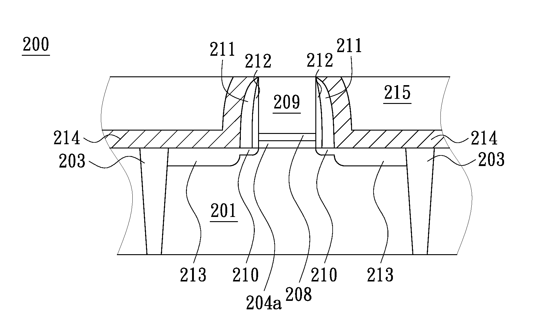
[0016]One object of the present invention is to provide a method for fabricating a semiconductor device to increase the yield of a FET with a high-k / metal gate structure.

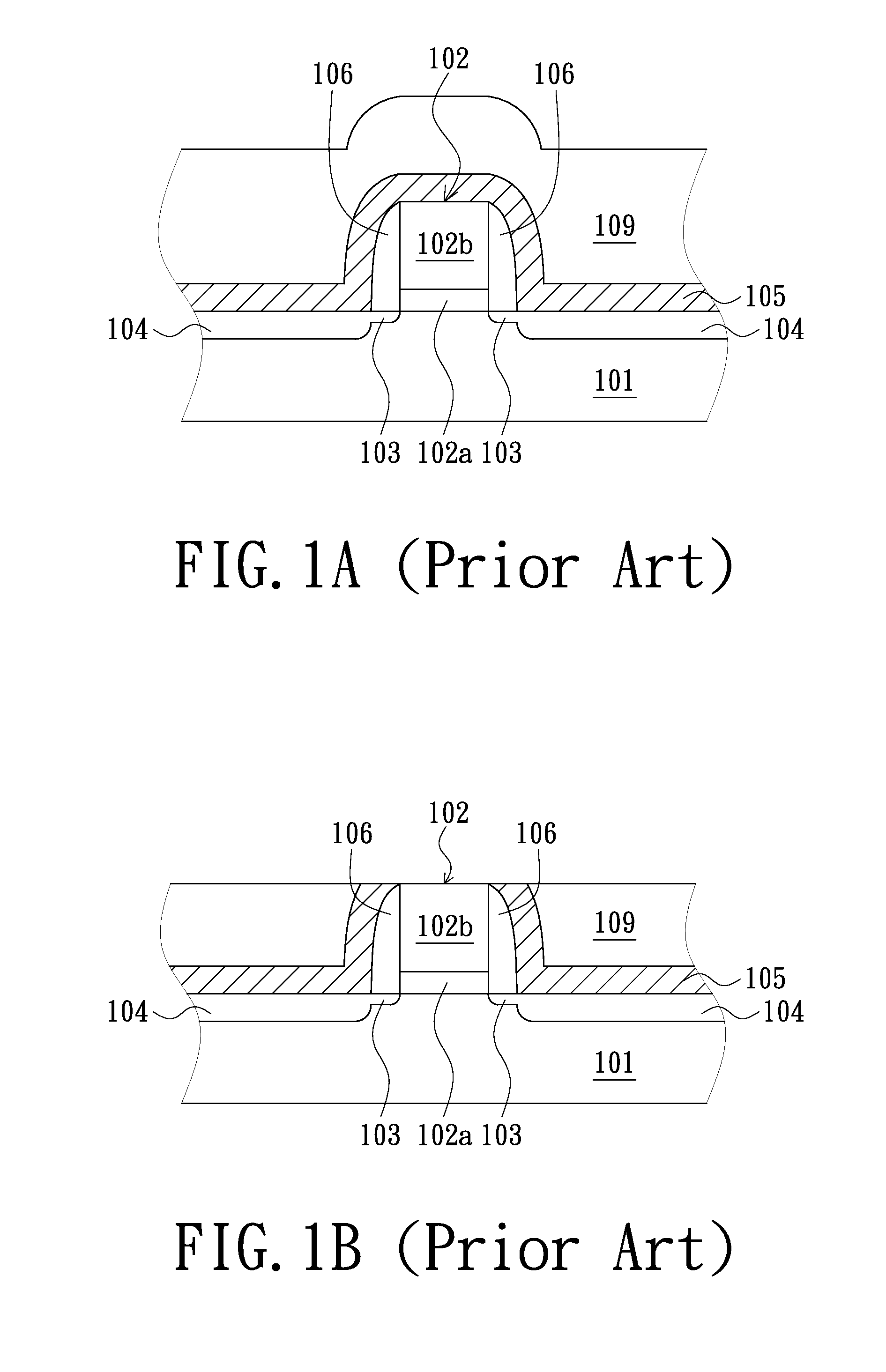
[0017]FIGS. 1A to 1D illustrate cross sectional views of the processing structures for fabricating a conventional high-k metal gate structure of a Field Effect Transistor (FET) 100. As shown in FIG. 1A, a dummy poly gate structure 102 comprising a gate dielectric layer 102a, a polysilicon gate electrode 102b and spacers 106 is formed over an active region of a substrate 101 in which lightly doped regions 103 and source / drain regions 104 are subsequently formed. Then, a contact etching stop layer (CESL) 105 and an interlayer dielectric (ILD) layer 109 are formed over the substrate 101 and the dummy poly gate structure 102.

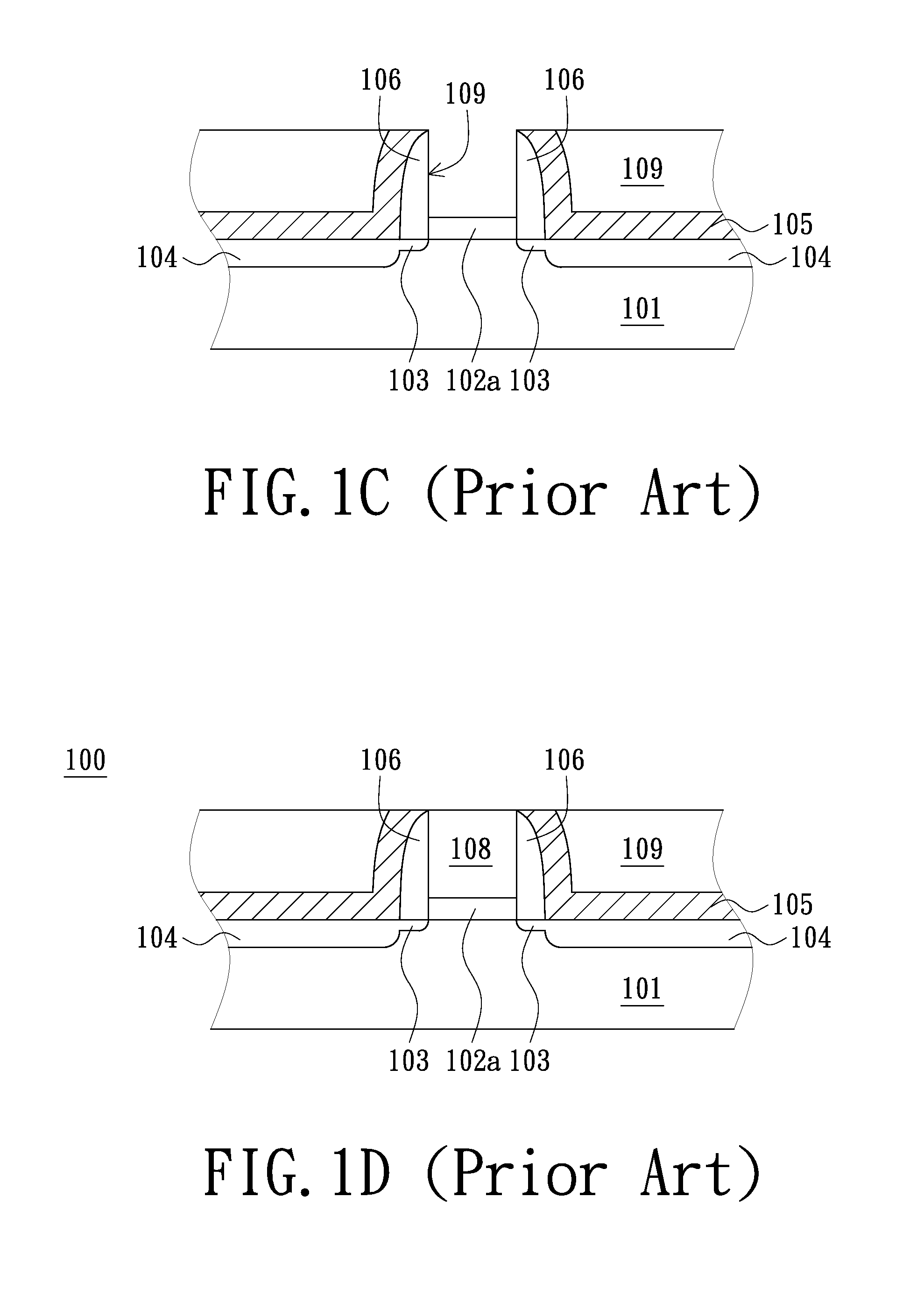
[0018]Next, a chemical machine polish (CMP) process is conducted to planarize the CESL 105 and / or the ILD layer 109 until a top portion of the dummy poly gate structure 102 is exposed as shown in FI...


PUM


Abstract

A method for fabricating a semiconductor device, wherein the method comprises steps as follows: a semiconductor structure comprising a substrate, a dummy gate structure having a dielectric layer disposed over the substrate and a silicon layer disposed over the dielectric layer, and an etching stop layer (ESL) and an inter-layer dielectric (ILD) layer both of which are sequentially disposed over the substrate and the dummy gate structure is first provided. Then, a chemical mechanical polishing (CMP) is performed to planrizing the ILD layer and expose the ESL. Subsequently, an in-situ etching process is conducted to remove portions of the ESL and the silicon layer to form an opening in the dummy gate structure. Next, metal material is filled into the opening.

Description

FIELD OF THE INVENTION[0001]The present invention relates to a method for fabricating a semiconductor device, more particularly to a method for manufacturing a field effect transistor (FET) with a metal gate structure.BACKGROUND OF THE INVENTION[0002]With the development of the electrical technology, a FET with high integrity and operation speed is required. As each technology nodes shrink, the dimensions of a FET and the thickness of its gate oxide, however, must be reduced and gate leakage could be more likely triggered by the reduced gate length.[0003]In order to reduce gate leakage, high dielectric constant (high-k) gate insulator layers are used and the conventional polysilicon gate electrode is replaced with a metal gate (MG) electrode to improve the device performance as the feature sizes has being decreased.[0004]However, there are still problems with the current fabrication approach of the high-k metal gate structure, thus to increase the yield of the FET is still a challen...

Claims


Application Information

Patent Timeline
IPC IPC(8): H01L21/28
CPCH01L29/4966H01L29/66545H01L29/7833H01L29/6659H01L29/6656
Inventor LU, SHUI-YENLIN, YI-POLIAO, JIUNN-HSIUNGTZOU, SHIH-FANGCHEN, SHIN-CHIN
Owner UNITED MICROELECTRONICS CORP
Why Eureka
Try Eureka