Multi-Junction Semiconductor Photovoltaic Apparatus and Methods

Inactive Publication Date: 2012-11-22
SIONYX
View PDF4 Cites 27 Cited by
  • Summary
  • Abstract
  • Description
  • Claims
  • Application Information

AI Technical Summary

Benefits of technology

[0007]Prom the discussion given above it can be appreciated that better photovoltaic devices are desirable. The following discussion provides such improved apparatus and methods of manufacture of the apparatus. Embodiments hereof provide a method of using laser processing to create at least a textured portion (e.g., an absorbing layer) within a multi-junction thin film silicon solar cell that increases the long wavelength light efficiency. More specifically, th

Problems solved by technology

However, to date, most thin-film technologies have lower efficiencies as compared to thick substrates.
The efficiency loss is mainly attributed to absorption losses and crystalline defects.
Reduced cost but lower efficiency becomes a hurdle to competing in large-scale power generation applications where there are surface area constraints and installation costs dominate the overall cost structure.
However, thin-films s

Method used


Image

  • Multi-Junction Semiconductor Photovoltaic Apparatus and Methods
  • Multi-Junction Semiconductor Photovoltaic Apparatus and Methods
  • Multi-Junction Semiconductor Photovoltaic Apparatus and Methods

Examples


Embodiment Construction

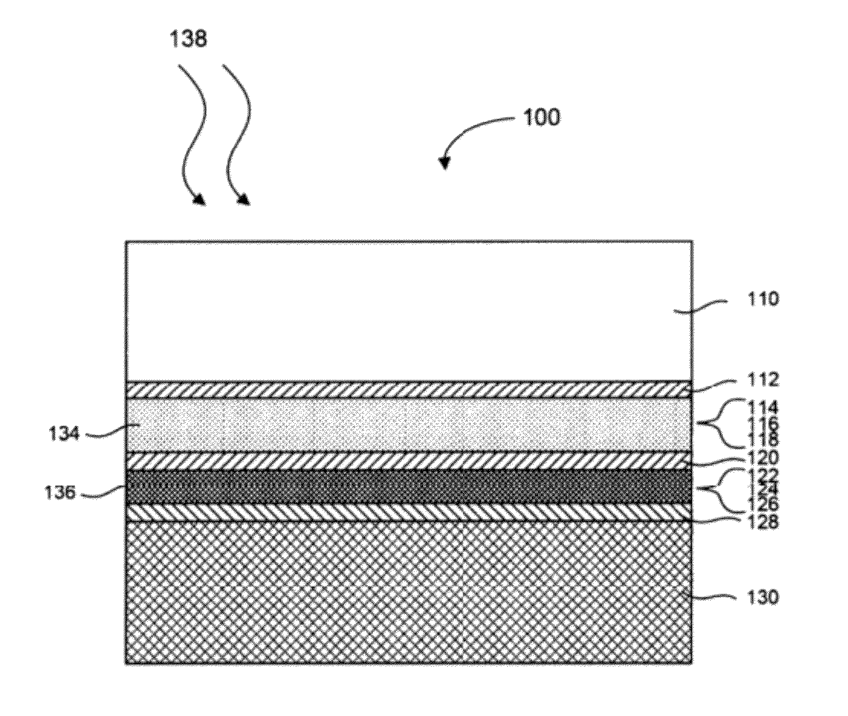
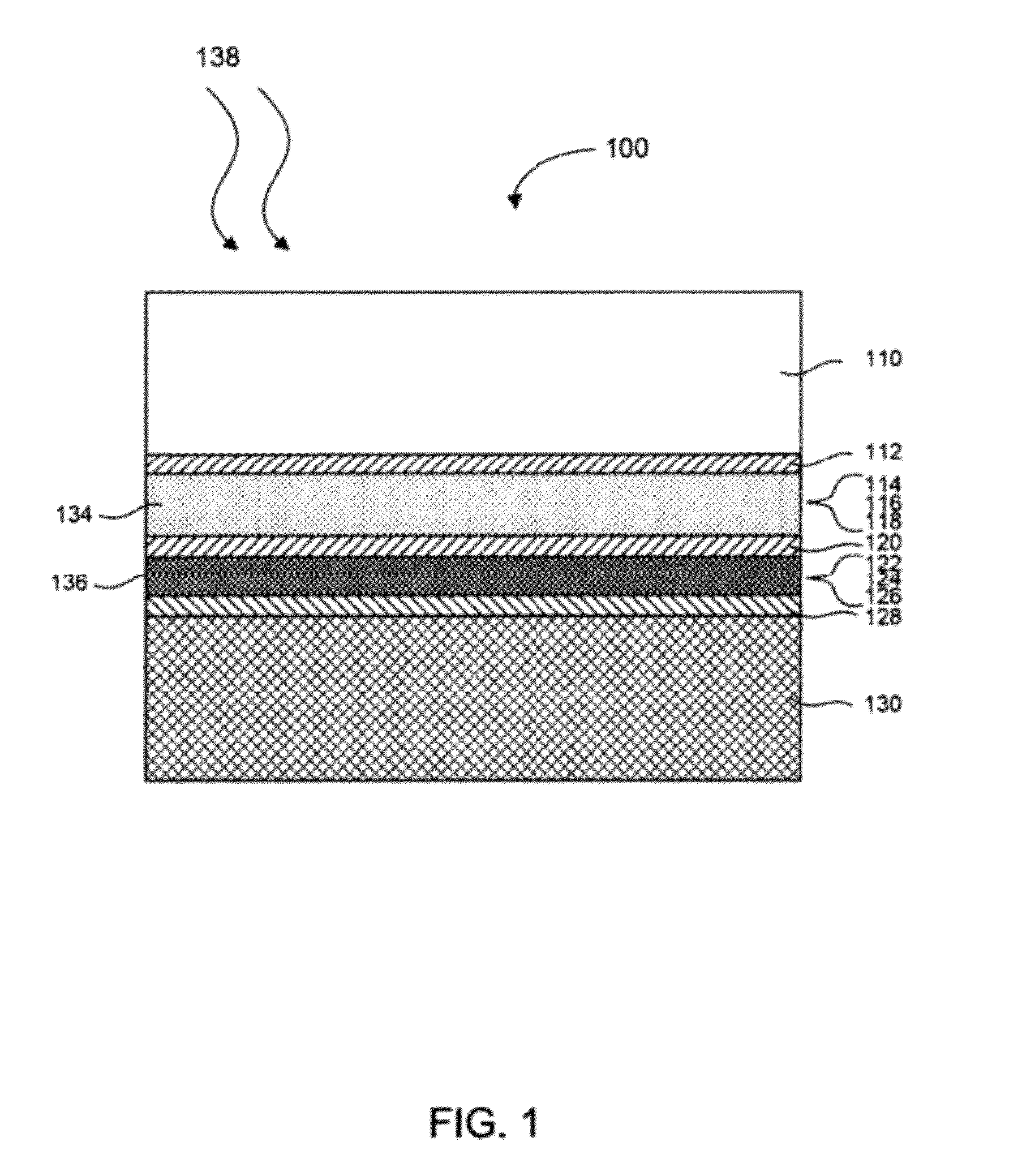
[0036]As disclosed above, the present invention describes systems and articles of manufacture for providing multi-junction thin-film semiconductor photovoltaic devices and methods for making and using the same. In some embodiments, the multi-junction thin-film semiconductor device can include at least one textured portion to enhance absorption characteristics of the device. The textured portion can include a conical structure or microstructure morphology. For example, the textured portion can include a Lambertian structure having micron-sized height variations. In some embodiments, the textured portion can be formed by laser-processing or by other known techniques.

[0037]In some embodiments, at least a portion comprising a semiconductor material, for example silicon, is irradiated by a short pulse laser to create modified micro-structured surface morphology that includes a textured portion. The laser processing can be the same or similar to that described in. U.S. Pat. No. 7,057,256,...


PUM


Abstract

A photovoltaic device and methods of manufacturing a photovoltaic device are disclosed. A photovoltaic device includes a first photovoltaic cell, a second photovoltaic cell, a semiconductor layer, and a doped layer. The second photovoltaic cell is in electrical communication with the first photovoltaic cell. The semiconductor layer includes a textured portion. The doped layer is configured to create a back surface field, the doped layer disposed between a proximal layer of the second photovoltaic cell and the semiconductor layer.

Description

TECHNICAL FIELD[0001]The present disclosure relates to the manufacture of photovoltaic devices. More specifically, the present invention is drawn towards thin film photovoltaic devices.BACKGROUND[0002]The advantages of thin film solar cells over “thick” cells include reduced material cost, large area and complete module processing, and the ability to be fabricated on flexible and transparent substrates. However, to date, most thin-film technologies have lower efficiencies as compared to thick substrates. The efficiency loss is mainly attributed to absorption losses and crystalline defects. Reduced cost but lower efficiency becomes a hurdle to competing in large-scale power generation applications where there are surface area constraints and installation costs dominate the overall cost structure.[0003]The most common material groups used in thin-film solar cells are silicon (amorphous and polycrystalline), cadmium indium diselenide (CIS and CIGS if gallium is included), and cadmium t...

Claims


Application Information

Patent Timeline
IPC IPC(8): H01L31/06H01L31/18
CPCH01L31/02363H01L31/076H01L31/1804Y02E10/547H01L31/206Y02E10/548H01L31/1864Y02P70/50
Inventor VINEIS, CHRISTOPHERPRALLE, MARTIN U.CAREY, JAMES E.
Owner SIONYX
Why Eureka
Try Eureka