Method for manufacturing semiconductor light emitting element, semiconductor light emitting element, lamp, electronic device and mechanical apparatus

Active Publication Date: 2012-12-27
TOYODA GOSEI CO LTD
View PDF2 Cites 14 Cited by
  • Summary
  • Abstract
  • Description
  • Claims
  • Application Information

AI Technical Summary

Benefits of technology

[0032]In this way, it is possible to form the second n-type semiconductor layer in which the second layer with low resistance is formed on the first layer with high crystallinity. Therefore, the resistance of the second n-type semiconductor layer is reduced, the crystallinity thereof is improved, and the flatness of the surface thereof is improved. In this way, it is possible to grow a light emitting layer (MQW layer) or a p-type semiconductor layer

Problems solved by technology

However, when the growth chamber for forming the n-type semiconductor layer and the growth chamber for forming the p-type semiconductor layer are separately provided

Method used


Image

  • Method for manufacturing semiconductor light emitting element, semiconductor light emitting element, lamp, electronic device and mechanical apparatus
  • Method for manufacturing semiconductor light emitting element, semiconductor light emitting element, lamp, electronic device and mechanical apparatus
  • Method for manufacturing semiconductor light emitting element, semiconductor light emitting element, lamp, electronic device and mechanical apparatus

Examples


example 1

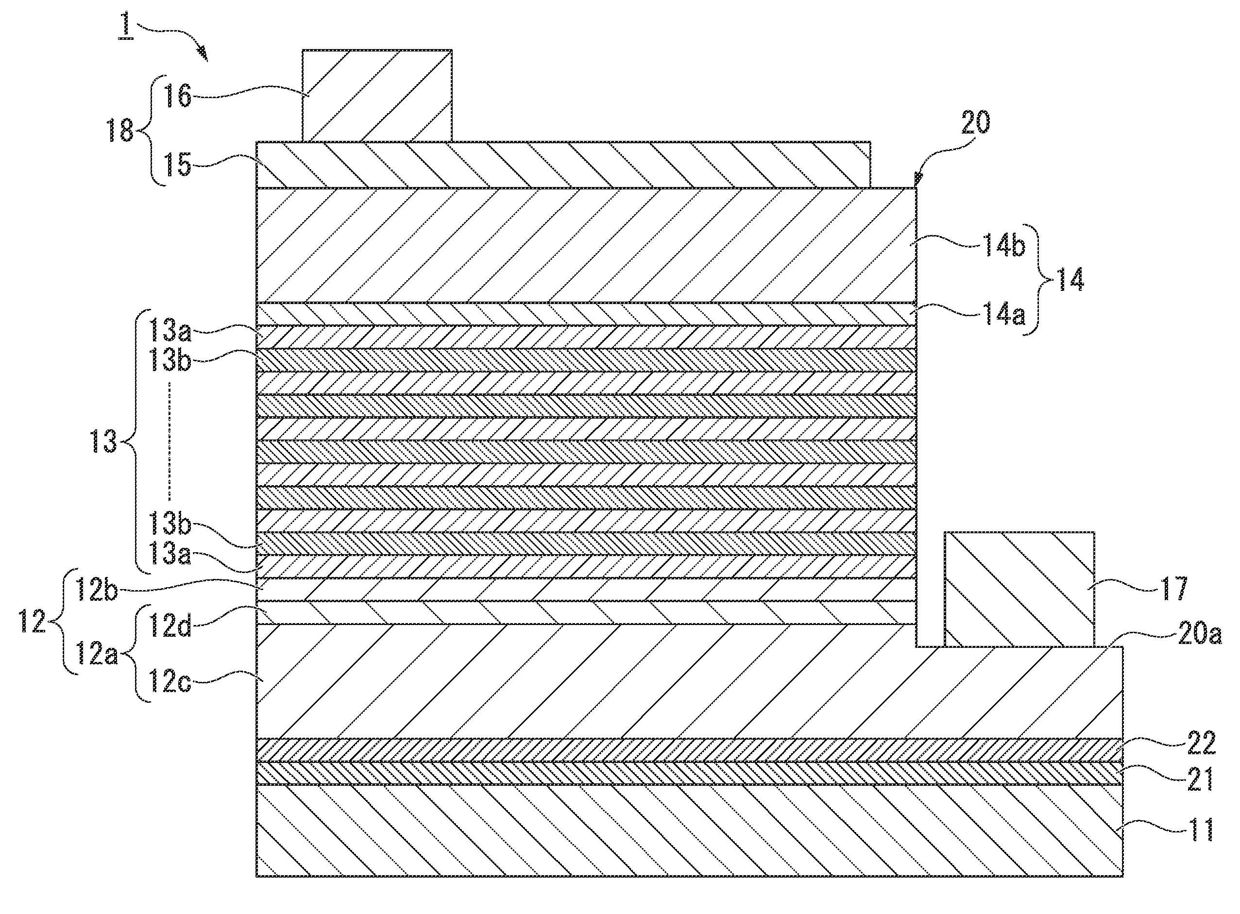
[0143]The semiconductor light emitting element 1 shown in FIG. 1 was manufactured by the following method.

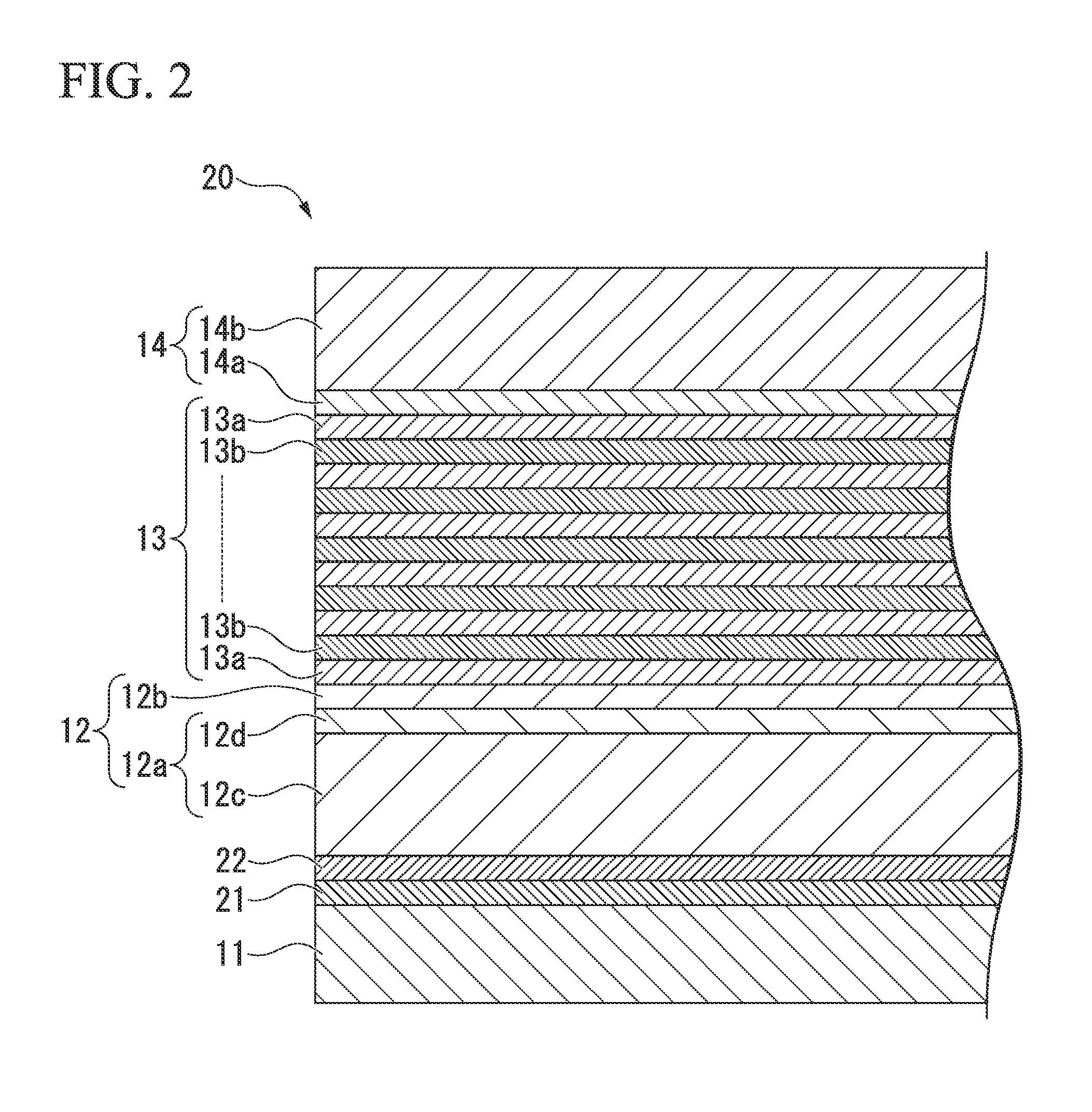
[0144]In the semiconductor light emitting element 1 according to Example 1, in a growth chamber of a first MOCVD furnace, a buffer layer 21 made of AlN, an underlayer 22 that had a thickness of 6 μm and was made of undoped GaN, and a first n-type semiconductor layer 12c that had a thickness of 2 μm and was made of Si-doped n-type GaN were formed on a substrate 11 made of sapphire.

[0145]Then, the substrate was taken out from the first MOCVD furnace and was then moved into a growth chamber of a second MOCVD furnace. Then, a heat treatment (thermal cleaning) was performed at 950° C. in an atmosphere including nitrogen and ammonium. Then, a regrowth layer 12d that had a thickness of 0.2 μm and was made of Si-doped n-type GaN was formed on the first n-type semiconductor layer 12c, thereby forming an n contact layer 12a with a thickness of 2.2 μm. The Si concentration of the n contact...

example 2

[0160]The same operation as that according to Example 1 was performed except that the Si concentration of the second layer of the second n-type semiconductor layer according to Example 1 was changed to 1×10¹⁹ / cm3 and the Si concentration of the interface of the second layer of the second n-type semiconductor layer with the light emitting layer 13 was changed to 1×10¹⁹ / cm3. The characteristics of a semiconductor light emitting element 1 were a forward voltage Vf of 2.9V, a light emission power Po of 24 mW, and a reverse current IR (@20 V) of 0.2 μA.

example 3

[0161]The same operation as that according to Example 1 was performed except that the first layer of the second n-type semiconductor according to Example 1 had a thickness of 40 nm and a Si concentration of 3×10¹⁷ / cm3, the second layer of the second n-type semiconductor layer had a thickness of 40 nm and a Si concentration of 7×10¹⁸ / cm3, and the Si concentration of the interface of the second layer of the second n-type semiconductor layer with the light emitting layer 13 was changed to 7×10¹⁸ / cm3. The characteristics of a semiconductor light emitting element 1 were a forward voltage Vf of 3.0 V, a light emission power Po of 23 mW, and a reverse current IR (@20 V) of 0.1 μA.


PUM


Abstract

Provided is a method for manufacturing a semiconductor light emitting element (1) in which a defect is less likely to occur in a light emitting layer and a p-type semiconductor layer due to the surface of a second n-type semiconductor layer and which is capable of obtaining a high output. The method for manufacturing a semiconductor light emitting element includes a first step of forming a first n-type semiconductor layer (12c) on a substrate (11) and a second step of sequentially forming a regrowth layer (12d) of the first n-type semiconductor layer (12c), a second n-type semiconductor layer (12b), a light emitting layer (13), and a p-type semiconductor layer (14) on the first n-type semiconductor layer (12c). In the step of forming the second n-type semiconductor layer (12b), a step (1) of supplying Si less than that forming the regrowth layer (12d) as a dopant to form a first layer of the second n-type semiconductor layer and a step (2) of supplying the Si more than that in the step (1) to form a second layer of the second n-type semiconductor layer are performed in this order.

Description

TECHNICAL FIELD[0001]The present invention relates to a method for manufacturing a semiconductor light emitting element, a semiconductor light emitting element, a lamp, an electronic device, and a mechanical apparatus, and more particularly, to a method for manufacturing a semiconductor light emitting element which is suitable when a large current is applied and applies a large current to obtain high light emission power, and a lamp, an electronic device, and a mechanical apparatus including the semiconductor light emitting element manufactured by the manufacturing method.[0002]Priority is claimed on Japanese Patent Application No. 2010-049628, filed Mar. 5, 2010, the content of which is incorporated herein by reference.BACKGROUND ART[0003]A semiconductor light emitting element which is used in, for example, a light emitting diode has been proposed. In the semiconductor light emitting element, an n-type semiconductor layer, a light emitting layer, and a p-type semiconductor layer ar...

Claims


Application Information

Patent Timeline
IPC IPC(8): H01L33/02
CPCB82Y20/00H01L21/0237H01L21/02458H01L21/0254H01L33/325H01L21/0262H01L33/007H01S5/3054H01S5/34333H01L21/02576
Inventor SAKAI, HIROMITSU
Owner TOYODA GOSEI CO LTD
Why Eureka
Try Eureka