Chemical Bath Deposition Apparatus for Fabrication of Semiconductor Films

a technology of semiconductor films and chemical baths, applied in the direction of liquid/solution decomposition chemical coatings, sustainable manufacturing/processing, final product manufacturing, etc., can solve the problems of power degradation, inapplicability of superstrate configurations on flexible workpieces on the basis of current technology, and serious problems to our environment, so as to save volume of waste solution, reduce waste treatment costs, convenient and economical preparation

Inactive Publication Date: 2013-01-03
WANG JIAXIONG
View PDF3 Cites 12 Cited by
  • Summary
  • Abstract
  • Description
  • Claims
  • Application Information

AI Technical Summary

Benefits of technology

[0012]The present invention provides a chemical bath deposition apparatus and the related method to fabricate semiconductor thin films in preparation of solar cells. It possesses a unique design to vertically transport a series of plane substrates side by side continuously through the whole apparatus. The deposition solution is continuously sprayed onto the substrate surfaces through a whole process from a freshly mixed to an aged stage. During the whole process, the backsides of all the substrates remain dry. The structure of this equipment is very simple and inexpensive for fabrication. In addition, the preparation of semiconductor thin films with this apparatus is economical. It also saves volumes of the waste solution to greatly reduce expenses of the waste treatment.
[0013]The present invention can be used for preparing thin film materials onto the surfaces of plane substrates via a CBD method. It is particularly useful to fabricate CdS or ZnS films in preparation of Group IB-IIIA-VIA and Group IIB-VIA thin film solar cells. In comparison with previous inventions, the presently invented apparatus and method should provide a more convenient and economical way in preparation of thin films through a CBD process.

Problems solved by technology

Moreover, the potential radiation contamination arising from the nuclear energy may bring serious problems to our environment, especially after the recent accident in a nuclear power station of Japan.
Besides, it has a problem of power degradation with initial illumination, but its technology is relatively mature.
However, a superstrate configuration may not be applicable on a flexible workpiece on the basis of current technology.
The disadvantage is that it produces lots of cadmium wastes and the post-treatment may be a heavy work.
However, Cd(OH)2 will dissolve in the ammonia alkaline solution to become [Cd(NH3)4]2+ complex cations and not affect the quality of the CdS product.
The reaction starting from a freshly prepared solution is not difficult to achieve in a laboratory work.
A lot of solution may be consumed and a waste treatment may be a very heavy work.
These applied forces may affect smooth movement of the flexible substrates.
It might be difficult to remain the surfaces flat, especially for a wide web.
It might always be a great challenge to remain backside of the substrates drying.
These apparatus and methods cannot be applied in a plane substrate since its edges are not able to be bent to maintain the solution on the front surface.

Method used


Image

  • Chemical Bath Deposition Apparatus for Fabrication of Semiconductor Films
  • Chemical Bath Deposition Apparatus for Fabrication of Semiconductor Films
  • Chemical Bath Deposition Apparatus for Fabrication of Semiconductor Films

Examples


example

A CdS Film Deposition for Fabrication of a CIGS Solar Cell

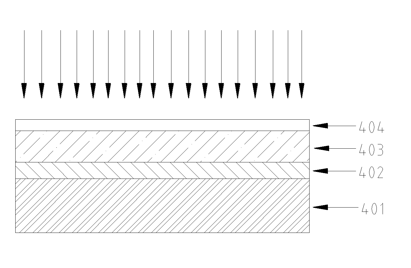
[0027]The present invention can be demonstrated with an example to deposit a CdS thin film on the surface of a CIGS absorber layer, as shown in FIG. 4. This figure is a schematic diagram illustrating the deposition of a CdS buffer 404 onto a CIGS absorber layer 403 that is coated on a piece of glass substrate 401 isolated with a Mo layer 402 as a back contact electrode. As an example, some 1.2×0.8 meter glass substrates coated with CIGS absorber layers may be used and delivered at a speed of 1 meter per minute. The main reaction chamber between the separation boards 117 and 116 is designed to be 12 meters long to meet a 12 minutes of reaction time. The conveyor belt may be fabricated with stainless steel and possesses frames to hold the substrates. The belt takes 2 seconds to load a substrate. If a CIGS surface is assumed to be covered with a 3 mm thick solution during the deposition, 3.6 liters of solution shall be consumed ...


PUM

PropertyMeasurementUnit
molar ratioaaaaaaaaaa
temperatureaaaaaaaaaa

Abstract

A chemical bath deposition method and a system are presented to prepare different thin films on plane substrates. In particular, they are useful to deposit CdS or ZnS buffer layers in manufacture of thin film solar cells. This method and the deposition system deposit thin films onto vertically travelling plane workpieces delivered by a conveyor belt. The thin films are deposited with continuously spraying the reaction solutions from their freshly mixed styles to gradually aged forms until the designed thickness is obtained. The substrates and the solutions are heated to a reaction temperature. During the deposition processes, the front surfaces of the substrates are totally covered with the sprayed solutions but the substrate backsides are remained dry. The reaction ambience inside the reactor can be isolated from the outside atmosphere. The apparatus is designed to generate a minimum amount of waste solutions for chemical treatments.

Description

FIELD OF THE INVENTION[0001]The present invention relates to a chemical bath deposition (CBD) apparatus and a method that can be used to deposit semiconductor thin films onto plane substrates. It is particularly useful for deposition of cadmium sulfide (CdS) or zinc sulfide (ZnS) semiconductor films for fabrication of thin film solar cells.BACKGROUND[0002]Photovoltaic technology has been developed under a background of global warming and exhausting of fossil fuels. The substitutes of traditional energy sources include nuclear energy and renewable energy. Among them, the nuclear energy will also be exhausted in the future. Moreover, the potential radiation contamination arising from the nuclear energy may bring serious problems to our environment, especially after the recent accident in a nuclear power station of Japan. Therefore, our future may greatly rely on renewable energy. The photovoltaic devices, or solar cells, are playing a leading role in the renewable energy. This enormou...

Claims


Application Information

Patent Timeline
Patent Type & Authority Applications(United States)
IPC IPC(8): H01L31/0296H01L31/0304B05B1/02H01L31/032B05C11/00H01L31/0272H01L31/0312
CPCC23C18/02C23C18/1204C23C18/1208H01L21/02485H01L21/02521H01L31/18H01L21/02628H01L31/0749H01L31/1828Y02E10/541Y02E10/543H01L21/02557Y02P70/50
Inventor WANG, JIAXIONG
Owner WANG JIAXIONG
Why Eureka
Try Eureka