Replacement metal gate with a conductive metal oxynitride layer

a metal oxide and oxynitride layer technology, applied in the field of metal oxidesemiconductor field effect transistors (mosfets) having metal gates, can solve the problems of increasing the effective oxide thickness, unable to achieve the effect of supplying the effective work function corresponding to the valence band edge of silicon, and difficult gate first integration schemes

Active Publication Date: 2013-01-10
IBM CORP
View PDF0 Cites 32 Cited by
  • Summary
  • Abstract
  • Description
  • Claims
  • Application Information

AI Technical Summary

Benefits of technology

[0005]A disposable gate structure and a gate spacer are formed on a semiconductor substrate. A disposable gate material portion is removed and a high dielectric constant (high-k) gate dielectric layer and a metal nitride layer are formed in a gate cavity and over a planarization dielectric layer. The exposed surface portion of the metal nitride layer is converted into a metal oxynitride by a surface oxidation process that employs exposure to ozonated water or an oxidant-including solution. A conductive gate fill material is deposited in the gate cavity and planarized to provide a metal gate structure. Oxygen in the metal oxynitride diffuses, during a subsequent anneal process, into a high-k gate dielectric underneath to lower and stabilize the work function of the metal gate without significant change in the effective oxide thickness (EOT) of the high-k gate dielectric.

Problems solved by technology

Controlling the threshold voltage of a metal-oxide-semiconductor field effect transistor (MOSFET) is one of the challenges in manufacturing a metal gate MOSFET.
Especially, providing a low threshold voltage for a p-type MOSFET having a metal gate has proven to be difficult for the gate first integration scheme, i.e., the conventional integration scheme in which the gate material is not subsequently replaced.
However, obtaining a material that provides effective work function corresponding to the valence band edge of silicon is still challenging.
Efforts to alter the work function of a metal layer by conventional thermal oxidation have resulted in an increase in effective oxide thickness (EOT), which degrades the performance of a metal gate MOSFET.

Method used


Image

  • Replacement metal gate with a conductive metal oxynitride layer
  • Replacement metal gate with a conductive metal oxynitride layer
  • Replacement metal gate with a conductive metal oxynitride layer

Examples


Embodiment Construction

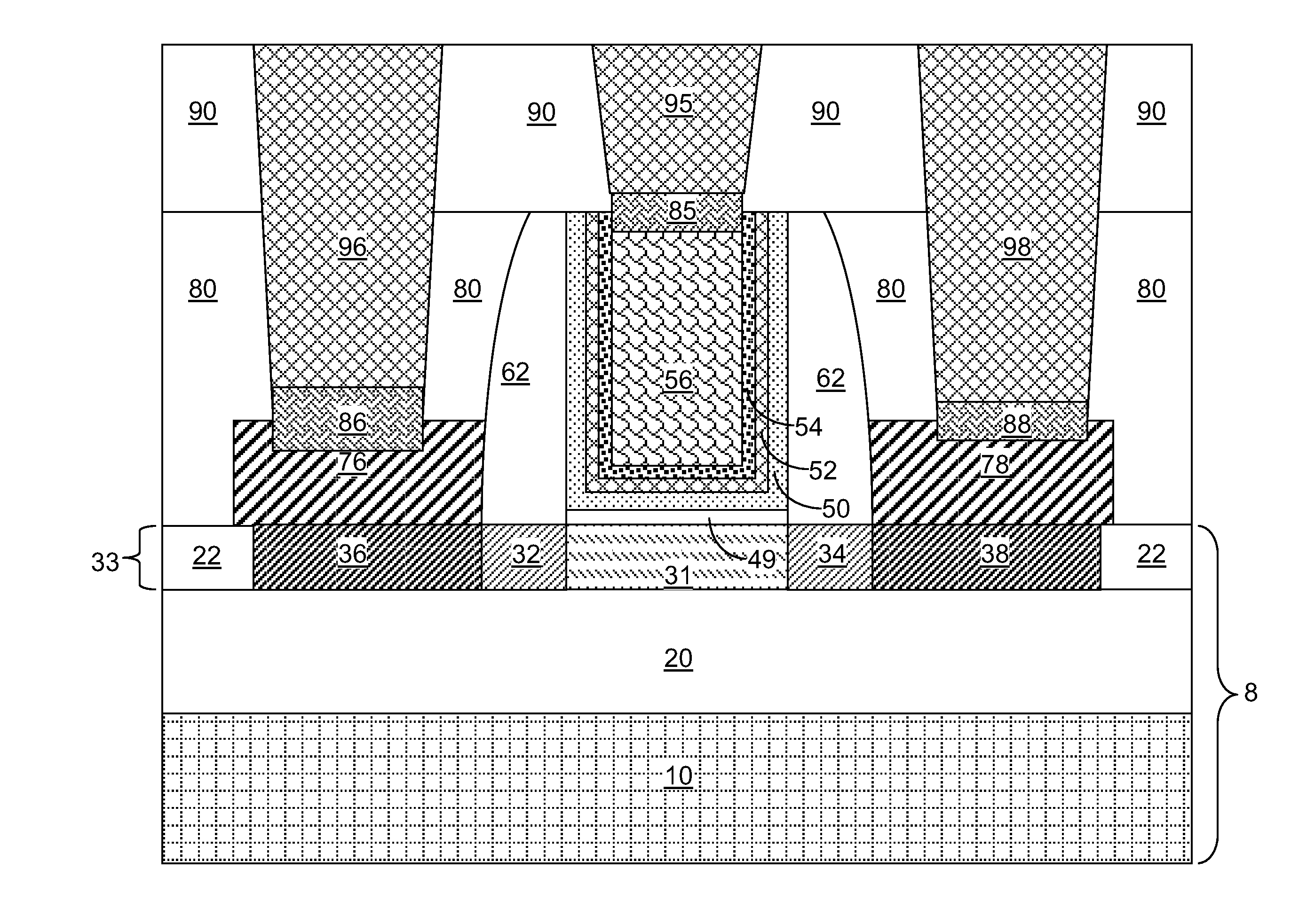
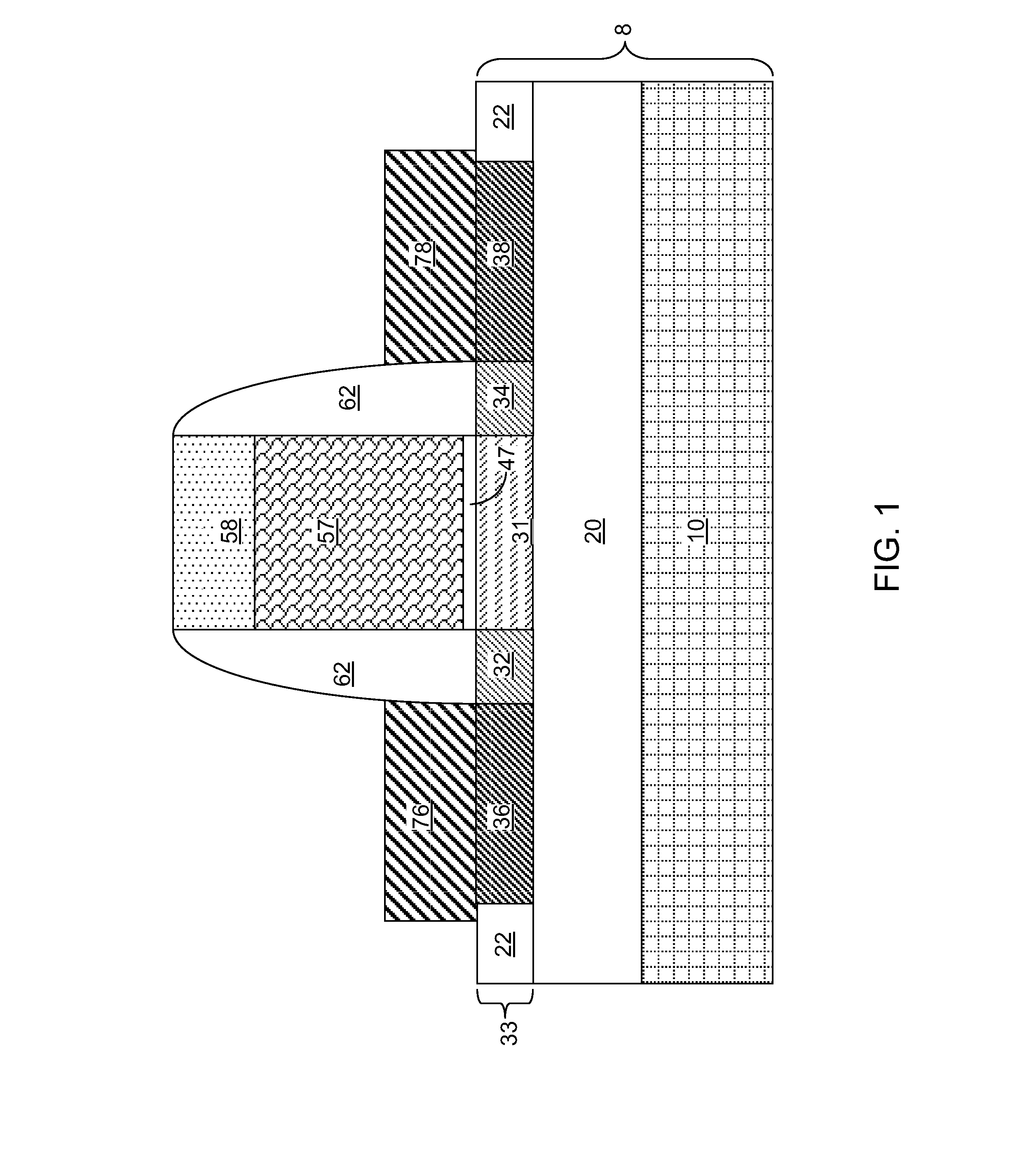
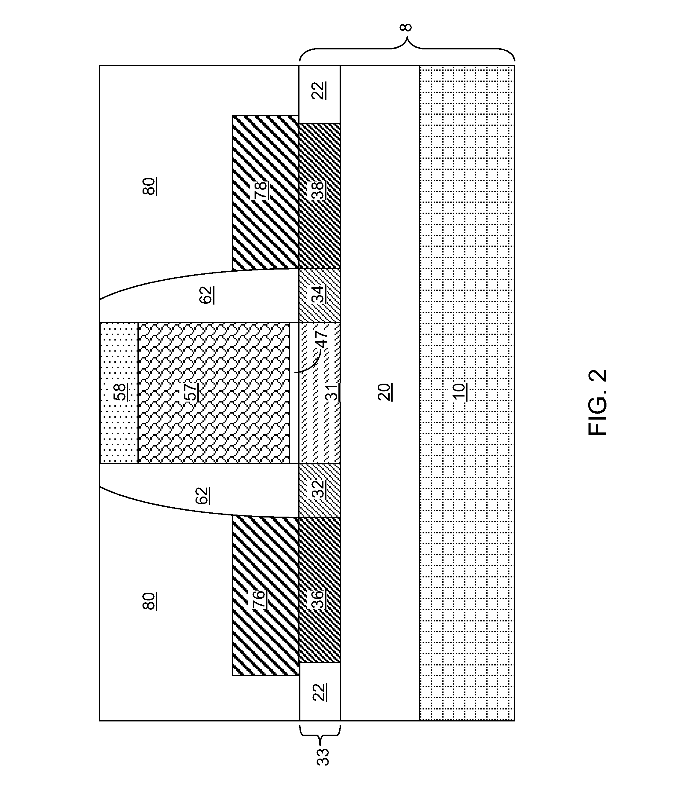
[0016]As stated above, the present disclosure relates to a metal-oxide-semiconductor field effect transistor (MOSFET) having a metal gate and methods of manufacturing the same, which are now described in detail with accompanying figures. Like and corresponding elements mentioned herein and illustrated in the drawings are referred to by like reference numerals. The drawings are not necessarily drawn to scale.

[0017]Referring to FIG. 1, an exemplary semiconductor structure according to an embodiment of the present disclosure includes a semiconductor substrate 8, which can be a semiconductor-on-insulator (SOI) substrate including a stack, from bottom to top, of a handle substrate 10, a buried insulator layer 20, and a semiconductor layer including a top semiconductor layer 33.

[0018]The handle substrate 10 can be a semiconductor substrate including a single crystalline semiconductor material such as single crystalline silicon, a polycrystalline semiconductor material, an amorphous semico...


PUM

PropertyMeasurementUnit
dielectric constantaaaaaaaaaa
thicknessaaaaaaaaaa
thicknessesaaaaaaaaaa

Abstract

A disposable gate structure and a gate spacer are formed on a semiconductor substrate. A disposable gate material portion is removed and a high dielectric constant (high-k) gate dielectric layer and a metal nitride layer are formed in a gate cavity and over a planarization dielectric layer. The exposed surface portion of the metal nitride layer is converted into a metal oxynitride by a surface oxidation process that employs exposure to ozonated water or an oxidant-including solution. A conductive gate fill material is deposited in the gate cavity and planarized to provide a metal gate structure. Oxygen in the metal oxynitride diffuses, during a subsequent anneal process, into a high-k gate dielectric underneath to lower and stabilize the work function of the metal gate without significant change in the effective oxide thickness (EOT) of the high-k gate dielectric.

Description

BACKGROUND[0001]The present disclosure relates to semiconductor structures, and particularly to a metal-oxide-semiconductor field effect transistor (MOSFET) having a metal gate and methods of manufacturing the same.[0002]Controlling the threshold voltage of a metal-oxide-semiconductor field effect transistor (MOSFET) is one of the challenges in manufacturing a metal gate MOSFET. Especially, providing a low threshold voltage for a p-type MOSFET having a metal gate has proven to be difficult for the gate first integration scheme, i.e., the conventional integration scheme in which the gate material is not subsequently replaced.[0003]The gate last integration scheme that employs a replacement gate remains an alternative. However, obtaining a material that provides effective work function corresponding to the valence band edge of silicon is still challenging.[0004]Efforts to alter the work function of a metal layer by conventional thermal oxidation have resulted in an increase in effecti...

Claims


Application Information

Patent Timeline
Patent Type & Authority Applications(United States)
IPC IPC(8): H01L29/78H01L21/336
CPCH01L21/28088H01L21/28176H01L29/4966H01L29/513H01L29/78654H01L29/518H01L29/66545H01L29/66628H01L29/66772H01L29/517
Inventor ANDO, TAKASHINARAYANAN, VIJAY
Owner IBM CORP
Why Eureka
Try Eureka